Showing posts with label Intel FPGA (Altera). Show all posts

Monday, December 21, 2020

Generating a high resolution HDMI/DVI output from an FPGA using Double Data Rate I/O (VHDL Teletext Decoder Part 5)

Introduction

I've already shown how to add a VGA output to an FPGA, but a HDMI/DVI output is sometimes more useful, as they offer better compatibility with modern displays, and a much higher bit depth (8 bits of colour per channel) is possible without needing to add extra I/O pins for each bit like you would with VGA. I've implemented a HDMI output as part of the VHDL Teletext project, and the main benefit for that project is that the additional colours supported by Level 2.5 teletext can be generated by the FPGA.

HDMI/DVI are very closely related to VGA, the timings are essentially the same, and it is in fact possible to generate VGA and HDMI/DVI from the same internal signals simultaneously. There is very little difference between HDMI and DVI, but DVI is video only, whereas HDMI usually carries audio as well. Generating audio will not be covered in this article, but any HDMI display should be able to accept a signal without audio, so the implementation in this article can be used for both and the only thing that differs is the choice of connector (the electronics are identical). The interface will be referred to as DVI from here on.

How does HDMI/DVI differ from VGA?

DVI is essentially the digital version of VGA. The main features are:

  • Analogue video channels are replaced by TMDS-encoded digital channels
  • Sync pulses are replaced by special codes that never appear in the active video area
  • Timings can be the same as VGA - timings are broadly categorised as "TV timings" and "PC timings"
  • Current-mode signalling is used on the hardware level
  • Data clock is 10 times the pixel clock, so a high clock speed is needed, but I'll address this issue by using Double Data Rate I/O

This diagram explains how the control signals work for a DVI video signal. Notice how the diagram is very similar to the equivalent diagram for a VGA interface.

Diagram showing the control signals for a DVI video signal

"TV timings" vs "PC timings"

Early HDMI TVs usually only support TV timings, and computer monitors and later TVs usually support all timings (computer monitors may not support interlaced timings, but those are outside the scope of this article). Examples of TV timings are 576p (720x576@50Hz), 720p (1280x720@50Hz and 1280x720@60Hz) and 1080p (1920x1080@50Hz and 1920x1080@60Hz) - 720x576@60Hz is not a proper TV timing, and will not be accepted by most older HDMI TVs. Examples of PC timings are 800x600 and 1280x1024, and PC monitors will often accept any clock frequency you make up as long as the refresh rate is within a certain range such as 50Hz to 80Hz. The most common values for the vertical and horizontal front porch, sync, and back porch for your chosen resolution can be found online (e.g. VESA Monitor Timing Standard).

An additional complication that affects TVs is the RGB Range, which can be "Full range" (0 to 255) or "Limited range" (16 to 235). TVs normally use "Limited range", but unless accurate colour is important, this generally doesn't matter for FPGA applications, especially text-only ones. Limited range was originally used for broadcast applications to avoid clipping analogue signals containing overshoots when they are converted to digital, which could introduce artefacts such as ringing if the digital signal is converted back to analogue.

Timings (EDID) can be read from the connected monitor over an I2C connection. The FPGA Teletext board includes the necessary connections to do this, but this hasn't been implemented in the firmware.

The TMDS signal

Digital video data is encoded using a scheme called TMDS (Transition-minimized differential signaling). It is a similar concept to 8B10B encoding, except the goal is to reduce the number of transitions rather than increase them.

The details of the algorithm are contained within the DVI specification, so I won't explain that in great detail. The algorithm is designed to be relatively easy to implement in programmable logic and in ASICs.

Another detail is that current-mode signalling is employed, whereas FPGAs usually have LVDS outputs, which use voltage-mode signalling. A limited selection of FPGAs have CML outputs, but for those which don't, a converter IC such as the PTN3366 can be used. Using LVDS directly will probably work at low resolutions using a short cable, but I wanted to do it properly on the FPGA Teletext PCB, so I used the PTN3366.

The code

The code is made up of these main parts:

  • Port definitions: the input for each channel is 8 bits, but if the input signal uses fewer bits, you can simply duplicate the bits to generate 8 bits for each channel. VHDL Teletext offers the user choice of two resolutions, so a selector input is provided for that. Pixel clock and high-speed clocks (5x pixel clock) are required.
  • Counter: controls the active area and pixels
  • Sync generator: determines whether the HSync, VSync, both, or no sync control codes should be used according to the counter values and resolution selection
  • TMDS encoders: three identical encoders for the three channels
  • Shifter: serialises the TMDS data using the high-speed clock

High-speed serialiser

The shifter is the part which differs from most HDMI implementations - the shifter is a shift register which shifts two bits per clock cycle, and two bits are extracted from each shift register to feed to the FPGA pins - this is for the Double Data Rate I/O.

DDR shift register block diagram

Shifting two bits per clock cycle allows the high-speed clock to be halved compared to the conventional method, which allows a dramatic increase in the maximum resolution without breaking the FPGA's maximum clock speed limit (402.5MHz for the PLL output on the MAX 10). This allows an increase in the maximum resolution from 800x600 to 1280x720. Even if the higher resolutions are not required, this still makes timing closure much easier, so is well worth doing regardless of what resolution you want to use. The impact on power consumption is minimal.

The values in the datasheet under "True LVDS Transmitter Timing Specifications" should also be considered. In the case of the VHDL Teletext board, the FPGA has a limit of 640Mbps, and 1280x720@50Hz is under this limit, but 1280x720@60Hz is above this limit. 1280x720@60Hz is under the limit of the fastest speed grade, which is more expensive. In practice, 1280x720@60Hz works fine on the slower speed grade, but this may not hold true at temperature extremes! The data rate in Mbps is 10 times the pixel clock, even when using DDRIO.

Implementation on the MAX 10 FPGA

On the MAX 10, the GPIO Lite IP core is used to implement Double Data Rate I/O. On other FPGAs, a different IP core may be used, such as the ALTDDIO IP core. The IP core updates the I/O pin on both edges of CLK_VIDEO_BIT, with either bit 0 or bit 1 from the TMDS encoder's shift register selected depending on whether the edge was a rising edge or a falling edge.

Take care when specifying the input pins. On the GPIO Lite IP core, the correct order (from high to low) is the four upper bits (CLK_OUT(1), R_OUT(1)...) followed by the four lower bits (CLK_OUT(0), R_OUT(0)...). This wasn't clearly explained in the documentation and caught me out the first time!

Example output on real hardware

Captured using the FPGA Teletext PCB:

Screenshot of 1280x720 signal generated by the FPGA

The hardware

The FPGA Teletext PCB, shown below with the numeric keypad removed, is a custom-designed PCB containing all the necessary hardware to decode the teletext data in a composite video signal (from a Raspberry Pi running vbit2 or from a satellite receiver) and display it on a HDMI or DVI display. The firmware could be used on other FPGA boards if the necessary external hardware is added.
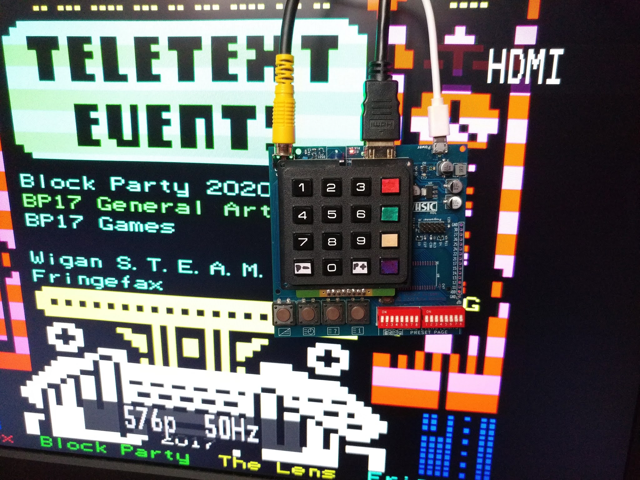
Photo of the FPGA Teletext PCB in action displaying a Teefax page

Please see the project overview for more details of the hardware, including links to buy.

Sunday, December 20, 2020

How to program Intel FPGAs over a network using OpenOCD on the Raspberry Pi (VHDL Teletext Decoder Part 4)

Introduction

Often, the need to program an FPGA without the proper programmer arises because programming needs to be carried out remotely, by a customer, or on a one-off basis where the cost of the proper programmer cannot be justified. Most of the guides online cover Xilinx FPGAs, with little attention given to Altera, and I felt that an Altera/Intel FPGA programming guide was necessary, so I've decided to write this entry which explains how to program a MAX 10 FPGA using a Raspberry Pi.

These instructions are aimed at the FPGA Teletext board, but are valid for any MAX 10 FPGA board.

The method described here will use OpenOCD. No external components are needed, and the programming can be done over an Ethernet connection. It has been tested on a first-gen Raspberry Pi and should be compatible with every model.

Programming the Flash with OpenOCD is slower than using the USB Blaster, and it takes a few minutes.

Setup

The first part of the procedure is identical to Adafruit's guide to programming microcontrollers using a Raspberry Pi. Connect your Raspberry Pi to your network and follow all of the instructions to compile and install OpenOCD. I would suggest setting up a connection to the Raspberry Pi using SSH if you have not already done this as it will make controlling the Pi much easier.

On the Raspberry Pi, create a new file called openocd.cfg using nano or another text editor, in your home directory, with the following contents:

source [find interface/raspberrypi-native.cfg]
transport select jtag
# The expected-id should be changed if you are using an FPGA other than the 10M08, you can find the IDs online
jtag newtap 10m08 tap -expected-id 0x31820dd -irlen 10
jtag_rclk 10000

Wire the Raspberry Pi up to the FPGA Teletext PCB's programming header using jumper wires. Use 100-ohm series resistors to protect the I/O against mishaps if you're not confident.

TCK TMS TDI TDO
Raspberry Pi header pin number 23 22 19 21
Raspberry Pi GPIO number 11 25 10 9
Altera/FPGA Teletext Decoder
programming header pin number
1 5 9 3

Don't forget to connect GND on the FPGA Teletext PCB (pins 2 or 10 on the programming header) to the Raspberry Pi.

FPGA-Teletext board connected to Raspberry Pi using JTAG connections

Programming the MAX 10 FPGA using the Raspberry Pi

On your computer, in Quartus, open the relevant programming file in the Programmer (POF for Flash programming), then go to File > Create/Update > Create JAM, JBC, SVF or ISC File. Make sure the file type is set to SVF, the operation is set to Program, and the speed set to something low like 1.0 MHz (the default of 25MHz is too fast for reliable operation with jumper wires). Move this file over to the Pi using PSCP.

Theoretically it should be possible to generate an SVF file from a SOF file and just program the SRAM, but I wasn't able to get this to work - programming would complete but the Flash (yes, the flash) would be erased.

Running this command will program the FPGA with the new design:

openocd -f openocd.cfg -c init -c "svf teletext-decoder.svf" -c shutdown

The new design should now be running on the FPGA.

If the Flash programming fails partway through the procedure, check that your jumper wires are making a good connection, then try lowering the clock speed when generating the SVF file. It would fail partway through the programming every time at the default frequency (25MHz) but it worked first time when I used 1MHz - the speed may need to be lower if using very long jumper wires.

Conclusion

This is a useful method for programming FPGAs with a Raspberry Pi. I see it as being especially useful for FPGA-based Pi Hats, where the FPGA can be permanently connected to the relevant pins on the Hat's connector, and also useful for products like the FPGA Teletext Decoder board where users are likely to own a Raspberry Pi but not a USB Blaster.

Next: Generating a high resolution HDMI/DVI output from an FPGA using Double Data Rate I/O

An alternative?

An alternative that's worth investigating: JTAG network programmer for Altera Quartus Prime. This should allow programming straight from the Quartus programmer and allow the use of SignalTap. When I tried it on an original Raspberry Pi, it was detected by Quartus, but the Raspberry Pi would freeze up completely whenever I tried to use it. I will experiment with it again on a newer model Raspberry Pi some time.

When trying that method, note that the pins on the header which need to be connected to the FPGA are different to the OpenOCD method, and after copying nw_jtag_srv to the Raspberry Pi, be sure to change its permissions using chmod 777 nw_jtag_srv.

Saturday, July 11, 2020

VHDL Teletext Decoder Part 3: Data recovery, processing and page extraction

In Part 2, I designed a display controller which can display a 40 character by 25 line screen of text and graphics as used by Teletext (and Mode 7 on the BBC Micro). The display controller reads from a dual-port RAM, which means it can be used in any FPGA project where data display and basic graphics are required. In the case of a teletext decoder, the VBI data needs to be extracted from the composite video signal, error correction needs to be applied, and then the data relating to the currently selected page number needs to be loaded into the dual-port RAM so that it is displayed by the display controller.

RTL block diagram

The teletext decoder section of the design has been broken up into four modules:

  • TXT_DATA_RECOVERY: Detects the start of a packet (line) of teletext data and extracts the serial data
  • TXT_DESERIALISER: Converts the serial data to parallel
  • TXT_DATA_PROCESSOR: Performs error correction on the data and determines the page number and subcode of each packet received
  • TXT_MEMORY_CONTROLLER: Writes packets from the selected page number to the dual-port RAM

Parallel vs serial transmission schemes

Not to be confused with serial and parallel data, these terms refer to the order in which pages are transmitted in the VBI (Vertical Blanking Interval).

In a parallel mode scheme, a few lines from one page in a particular magazine are transmitted followed by a few lines from a page from another magazine and so on. This approach was favoured by UK broadcasters when teletext was broadcast here and is still used by TEEFAX. This scheme can be identified from the display of page numbers only from the current magazine in the rolling header when waiting for a page.

In a serial mode scheme, all packets transmitted belong to the page number and magazine of the last header packet transmitted. This approach is favoured by international broadcasters, and is identified by page numbers from every magazine being displayed in the rolling header.

More detailed information about these schemes is described in Annex B of ETSI EN 300 706.

TXT_DATA_RECOVERY

This module detects the start sequence of the packet then forwards the serial data onto the next module. The start of the packet is shown below:

To simplify the design and avoid the need for a high-speed ADC, the packet is simply digitally sampled, which means the module only has a single digital input. A high-speed comparator is the only active semiconductor required, although the user may have to adjust the trimmer pot RV1 when switching sources.

Composite video input and sampling circuit

The comparator converts the analogue signal into a digital signal suitable for the FPGA:

The data recovery module, along with the rest of the teletext decoder section, runs at 27.750MHz, four times the data bit rate. A SI5351 programmable clock source is used to generate this unusual frequency with great accuracy along with the unique video clock required by the VGA controller for each resolution.

There are four sampled bits per data bit (known as 4x oversampling), and the bit rate has a very tight tolerance so there is no need to worry about clock recovery, which simplifies the design a lot. A shift register is continuously fed with the digital data provided by the comparator and a packet is detected once the start sequence is detected in the shift register. One out of every four bits will be sampled during the inter-bit transition, so the comparison is performed using only three sampled bits in every data bit, then the data sent to the next module is recovered from the middle sampled bit of each subsequent data bit.

Start pattern in teletext waveform

The colour burst is not sampled, nor is the video line number counted. These are not necessary for decoding, and the only consequence is the decoder will be capable of receiving anything transmitted otherwise in accordance with the specification which may be rejected by a commercial decoder.

TXT_DESERIALISER

This module converts the recovered data from serial to parallel. The FRAME_VALID_OUT signal indicates the start and end of each packet received to the next module.

TXT_DATA_PROCESSOR

This is the most complex module in the teletext decoder.

Page number detection

The two main types of packet are page header and normal packets. There's also non-displayable packets, but those will be explained later.

Teletext packet types

Every packet contains the magazine number, which is the leftmost digit of the three-digit page number, however, only the header packet contains the remaining two digits of the page number and the subcode. When a parallel transmission scheme is used, pages from different magazines may be transmitted on different lines in the same video frame, which means that the data processor must remember the page number and subcode of the last transmitted header packet for each of the 8 magazines. This is stored in the PAGE_AND_SUBCODE_CACHE whenever a header packet is received and retrieved whenever a packet other than a header packet is received so that the correct page and subcode is always sent to the next module along with the decoded data.

Packet processing

Hamming coding is used to protect certain data such as the page number and subcode to improve the chances of the header packet being decoded correctly in cases of poor reception. This reduces the chance of an incorrect page being loaded on top of the displayed page when a subsequent header packet is incorrectly determined to have the selected page number. Unfortunately, Hamming code dramatically increases the number of bits taken up by each piece of data, so it is only possible to use it for the most important data, and the display data is only protected with a simple parity check with no error correction capability because it is less critical that every display byte is correctly decoded. It should be noted that correct decoding of every single display byte is expected when the signal quality is good and there is no interference.

The parity checking and Hamming decoding is carried out by sub-modules (VHDL components) in TXT_DATA_PROCESSOR.

TXT_MEMORY_CONTROLLER

This module selects the appropriate address in the dual-port RAM to write each packet belonging to the specified page number to, then forwards the packet data on to the dual-port RAM.

It also controls the display of the status line. The last 8 characters should be continuously updated regardless of the magazine of the header row, whilst the rest of the header row should only be updated when waiting for a newly-selected page number ("search mode"), in which case only header rows from the current magazine should be displayed when the pages are transmitted using the parallel transmission mode, and header rows from all magazines should be displayed when pages are transmitted using the serial transmission mode.

This module also extracts the editorial links (also known as Fastext) for the four coloured buttons and the index button from the relevant non-displayable packet.

The 8 characters in the top left corner of the display are called the status characters. These are controlled by the keypad controller, and are used to display the page number and subcode number. The memory controller monitors these characters and updates the dual-port RAM whenever they change. The UPCOMING_FRAME_IN signal ensures that page content updates (which must happen in real-time) are prioritised over updates to the status characters.

The REQ_SUBCODE_SPEC_IN signal is set when the user requires a specific sub-page to be displayed. When the Time-Text button is pressed, the keypad controller sets the REQ_SUBCODE_SPEC_IN signal and the memory controller will then only display pages where both the page number and subpage match the requested values, otherwise the subpage is ignored and all subpages from the current page will be displayed as they are received.

Screenshot of the project in operation

The project can decode pages generated by VBIT2 running on a Raspberry Pi.

Teletext decoder connected to a display, showing a teletext page

Next: Data recovery, processing and page extraction

Saturday, April 18, 2020

VHDL Teletext Decoder Part 2: Page Display including Text and Graphics

In Part 1, I designed a very simple VGA controller, but without any content to display, it's not very useful. The next part that's required is the display controller, which is responsible for drawing the text, graphics and colours on the display.

The Display Controller shall take its input from the read side of a dual port RAM, which shall be written to by the Teletext Data Processor in this project, but the Teletext Data Processor could easily be replaced with something else for non-Teletext applications. A Display Controller based on the Teletext specification makes an excellent FPGA display generator, even for non-Teletext applications. This is because the specification was designed in the 1970s to be relatively easy to design an ASIC around, which means that the compiled logic size is very small compared to modern FPGAs, and makes it very "cheap" in terms of resources to add the display generator to any project.

This is generated entirely by an FPGA

Level 1 Teletext supports text and graphics via a character generator ROM, mosaics of 2x3 pixels, and selectable background colour.

Key display features

Text

The font used was taken from the datasheet for the Texas Instruments SN74S262N CGROM, originally used in the 1970s "Tifax" decoder design, and entered into a VHDL file.

The CGROM has a row output format, which is better than column output for horizontal-scanning display systems because the input address only has to change once for each character along the line currently being drawn rather than for every pixel.

Graphics

Basic graphics capability is provided by 2x3 mosaic tiles:

Careful examination of the mosaics set will reveal that each of the six tiles in the mosaic correspond to particular bits of the address. No additional CGROM is required, and the logic to draw the mosaics ends up being very simple. The addresses marked (1) are displayed from the CGROM; this allows CAPITAL LETTERS to be mixed in with mosaic graphics without having to switch between text and mosaic modes.

Mosaics can be contiguous or separated; this is set using spacing attributes.

Double height text

Double height display can be enabled at any point on a line, and applies to any characters or mosaics drawn after the Double Height command up until the end of the line or a Normal Height command. If a Double Height command is used anywhere on a line, the entire line below is ignored (even below characters that aren't double height), which seems strange, but this simplifies the logic design. The CGROM glyphs are easily "doubled in height" by bit-shifting the row selector right by one bit when in double height mode, with just a little bit of extra logic required to correctly draw the second line.

Colours

The available colours are: White, Yellow, Cyan, Green, Magenta, Red, Blue, Black. All of these can be output using only one bit per channel (R, G, B). Black cannot be used as the foreground colour in standards-compliant Level 1.0 and Level 1.5 Teletext decoders, but most modern decoders will interpret it anyway. Not interpreting it does not make the logic simpler, but my decoder will be designed to not interpret it in order to stick as closely to the specification as possible.

Spacing attributes

All attributes are set using these commands. They are called "spacing attributes" because each one takes up a space on the display. Level 2.5 and 3.5 Teletext also supports non-spacing attributes which do not take up space on the display, but that is outside of the current scope for this project.

All attributes are described in detail in Section 12.2 of the ETSI EN 300 706 V1.2.1 Enhanced Teletext Specification.

Attributes can be "set-at", meaning they apply immediately, or "set-after", meaning they apply from the next character position onwards. Correct implementation is required to ensure the correct display of "held" mosaics. Hold mosaics is a feature which displays spacing attributes as a repeat of the last mosaic to enable seamless colour changes; without hold mosaics, spacing attributes would always be displayed as spaces and graphics like the famous Ceefax weather map would not be possible.

Mix and Reveal

The Conceal attribute hides text and mosaics. Setting the Reveal input high will display the hidden content.

The Mix feature on a real TV displays the foreground content on top of the TV picture. All background colours effectively become transparent. Currently, the design has no capability of drawing the text on top of an existing video signal, so all this function does at the moment is show all background colours as black. The Start Box and End Box attributes are unimplemented for the same reasons.

Firmware

The main parts of the logic are:

  • Combinational logic for mosaic generation
  • CGROM
  • Active area controller: Determines whether we're currently in the area of the screen where the content will be drawn using a set of constants which determine character height, display height and width, characters per line, and number of VGA pixels per Teletext pixel
  • Line and character counters: each pixel and each row within each character needs to be counted
  • Display generator: reads the dual port RAM data and interprets the spacing attributes
  • Logic to control setting the output signals to the foreground/background colours, and flashing

Teletext uses 40 characters and 25 lines, but the display controller is in no way constrained to that, and this can easily be changed using constants in the code for other applications.

Development

As the Display Controller operates independently of the Teletext decoding, development can be done without the decoder by loading a Teletext page into the dual port RAM by specifing it as the default data in Quartus. It is not possible to use .tti files directly because the spacing attributes are converted into ASCII sequences, and unnecessary header stuff is added, but it's simple enough to convert it to raw data by hand.

Here's the display from an early version of the display decoder:

A largely-completed display generator combined with working teletext decoder:

The firmware is available on GitHub

Despite making little attempt to "optimise" the code, the whole system including teletext decoding takes up only 6% of the small (to modern standards) 22k logic element Cyclone 10 LP FPGA.

Still to come...

Next: Data recovery, processing and page extraction

See all posts with the label Teletext to see my future progress on this project.

An additional challenge would be to design firmware to synchronise to an external VGA signal and draw text on top of the incoming VGA signal.

Large dot matrix clock, timer and scrolling message display

First completed: August 2014. Additional work carried out late 2025/early 2026. Introduction Previously, the author had made a very small ...