Sunday, March 15, 2020

Why does the cycle life of EEPROM and Flash need to be considered in your design?

Most microcontrollers nowadays come with up to a few kilobytes of EEPROM, and this memory is frequently used to store user settings and sometimes for basic logging. Flash-based microcontrollers have EEPROM because Flash memory must be erased in large blocks (pages) before writing, which is fine for program memory, but inconvenient for settings where only a few bytes need to be changed and storing a whole page in RAM to re-write may be inconvenient.

Here's the parameters for the various types of memory in a popular microcontroller:

One thing you may be quick to forget about is the number of write/erase cycles. "100,000 cycles, that's a big number, great, don't need to worry about it."

That is a bad approach. Cycle life is important; especially if you don't want your company to gain a reputation for making "landfill electronics", "lagdroid phones", or "cars that frequently need expensive electrical repairs out of warranty..."

I'm not going to demonstrate using a program which repeatedly writes the same location for ever more; I will focus on practical examples.

A practical demonstration

This is the Dashboard Display 1.0:

Using a GPS module, it measures the current speed, and the distance and time taken for each trip. I'll cover the project in more detail later. It's also the forerunner to the much more advanced project I did for my university dissertation, Global Positioning System and European On-Board Diagnostics-based Automotive Monitoring System.

The Dashboard Display was designed to be continuously powered, with connection to the vehicle via a short car radio extension cable with spliced-in cables running to the multi-pin connector on the front. These connections allowed the backlight to automatically come on and dim when required. The trip distance and time were stored in EEPROM just in case the power was disconnected, however.

The power was disconnected after six months, and this is what came up when power was restored:

How did that happen? My first guess was that I had made a type casting error in C, but that error usually results in losing 1s off the left of a variable, not gaining them. Additionally, the problem came back after resetting the trip counter and cycling the power again.

I examined my code and found that it saved the time and distance to EEPROM once a second, even when the trip counter was not running (it paused itself whenever no movement was detected). As a result, the same eight EEPROM locations were written around 15000000 times, or 150 times the maximum rating. I wrote a little test program to test it, and these 8 locations were well and truly banjaxed, being unable to hold the freshly written data for even the few microseconds it took for my program to read back the values.

All 8 bytes were affected, since the microcontroller cannot erase individual bits, and does not have the intelligence to not erase unchanged bytes unless programmed to check them. Interestingly, the bytes still passed testing when a sequence of 11111111 was written, and only failed when patterns of alternating bits were written, suggesting that neighbouring bits influence failing bits. The failing bits were always read back as 0 when alternating bit sequences were written.

Where was the mistake made?

It's easy to put the blame on the piece of code which was supposed to not write the trip values when the trip counter was paused but didn't, but that's the wrong attitude. It's true that the EEPROM would have suffered much less wear had that mistake not been made, and it would have taken a much longer time for any problems to surface, but the mistake was in fact the decision to write the trip data every second. That decision was made to ensure accuracy of the data should power be lost temporarily, with no consideration made for longevity. Had the code been written correctly (according to specification), it would have needed only 27 hours of continous driving to exceed the rated lifespan of the EEPROM. The rated lifespan is usually worst case (highest voltage and temperature), but this should not be acceptable.

The frequency of saving data to EEPROM must be carefully considered when designing a product. In this case, it's unlikely that power would be lost mid-trip, and it would probably be acceptable to save the data only when the trip is stopped or reset, which is how the Global Positioning System and European On-Board Diagnostics-based Automotive Monitoring System handles this problem.

If you really need to write often

With ever increasing flash memory density and cost pressures, the cycle life of flash memory can be as low as 1000 cycles. Wear levelling is a technique used by modern flash-based mass storage and works well as long as there is a good amount of "unused" space. This technique can also be used on a microcontroller, but is not without its challenges.

Other solutions include using FRAM, which is similar to EEPROM except with practically unlimited cycle life, and battery-backed SRAM.

But the best solution is to minimise how often you write data. And if you're writing logging data, do you really need to?

A commercial example

Here's an example of how such a simple oversight can affect even the biggest companies:

Photo by Tokumeigakarinoaoshima - licensed under CC BY-SA

The MCU is the main computer in Tesla cars, and it uses eMMC Flash memory. The software writes a lot of logging data, and this in conjunction with the relatively small 8GB Flash chip results in the Flash getting worn out in just a few years on heavily used cars. The only official repair is replacement of the MCU costing £2500+ out of warranty.

At least in this case, this problem can be mitigated somewhat with software updates. Many embedded projects do not have that luxury.

Learn more about this issue here: https://teslaownersgroup.co.uk/kb/emmc-chip-failure-what-is-it-should-i-be-worried-what-can-i-do

Do you know of any other commercial examples? Let me know in the comments.

Friday, February 21, 2020

Experimenting with a programmable RF Modulator (making a controller for it and testing harmonics)

I was scavenging two old Sky boxes for parts, and although the very large scale integration of the mid-noughties set-top boxes meant there was very little worth removing, I did extract two of these RF modulators.

RF Modulators convert composite video and audio into an analogue TV channel that can be received on any television set and combines it with the signal from the RF input, enabling the picture from the Sky box to be received on every TV set in the house in addition to the off-air channels. Sky RF modulators are unique in that they have two outputs, one of which features line power and a low-frequency return path to support the "digilink" system, which allows the Sky box to be controlled from the other TVs. See diagram of this setup. This blog entry, however, will focus on the RF output rather than those additional features.

The modulator is completely shielded, but the shielding clips off easily to expose the insides. Much like the rest of the Sky box, the modulator is very highly integrated, and it uses a Freescale MC44BS373CA single chip solution. Impressively for a design which handles signals of up to nearly 1GHz, the modulator is built on a single-layer PCB, presumably to keep costs low. The circuit appears to be largely based on the application circuit in the datasheet, with the addition of some passives and transistors to handle the line power injection, IR return path, and amplification of the RF input. The 75-ohm termination resistor on the video input is missing.

The MC44BS373CA is frequency-agile, which means it can be programmed to work at different frequencies, all the way down to 45MHz in fact. Despite this, the Sky box only allows selection of UHF channels, despite VHF System I still being used in Ireland, so let's find out why not...

Programming the modulator

The modulator has a very simple I2C interface documented in Table 8 in the datasheet, and it supports 5V and 3.3V operation, allowing easy interfacing to Arduino, Raspberry Pi, etc.

The controller is supposed to have a programmable I2C address, but this feature is not available on the package used in this modulator, so it is fixed to 0xCA (8-bit).

There's not a lot of settings that can be configured. The main settings of interest are the oscillator frequency (N11:N0), divider (X2:X0), and test pattern enable (TPEN). The sound frequency bits (SFD1:SFD0) should simply be set to the appropriate setting for the region (10 for System I).

The relationship between frequency, divider and N11:N0 is simple, and I've put it into a table here:

X2:X0 (Divider) N11:N0 F (MHz)
000 (1) 4F N/4
001 (2) 8F N/8
010 (4) 16F N/16
011 (8) 32F N/32

The oscillator is rated for 460MHz to 880MHz, so it's necessary to use the divider to use lower frequencies.

Example project

I made an Arduino sketch to control the modulator. It allows selection of the channel number, from which the frequency and divider are automatically calculated, plus selection of the system (B, D, I, M) and the test pattern.

I haven't included a schematic because the wiring is very simple; all pins are defined in the code. The only important components to remember are the pull-ups on the I2C bus (hidden under the LCD) and the 75-ohm termination resistor between Video In and GND. Failure to include the latter results in horrendous close-spaced ghosting caused by signal reflection.

This controller was used to enable easy control of the modulator during testing.

Link to the code on GitHub.

Real-world testing

My current oscilloscope can only show the spectrun of signals up to 25MHz, so we can't look at the output spectrum, but what we can do is examine the output picture under various different test conditions.

The datasheet gives two figures for the minimum frequency in different places: 30MHz and 45MHz. The latter seemed to be true.

The programmable oscillator seemed to work down to about 400MHz, below which there was no output and it was necessary to up the divider. It worked fine up to 900MHz, the highest any TV I had went up to, so it may have gone even higher.

The single-sided board didn't seem to compromise the quality at higher frequencies.

The picture had lots of 'sparklies' when using the highest divider (16). It's not needed to access the lowest frequencies anyway.

Harmonics

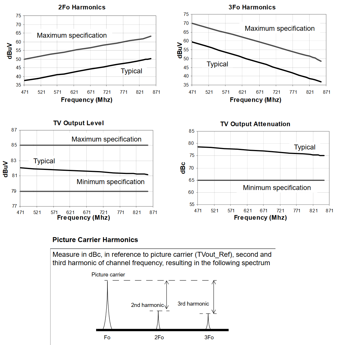
What parts are of particular interest? These graphs...

Look at the signal levels of those harmonics. Unlike this newfangled digital stuff, analogue TV is very suspectible to interference, and a signal to noise ratio of 46dB is required for noise-free viewing. These harmonics result in a signal to noise ratio well below that at affected frequencies, which will spoil anything on those frequencies. The 2nd harmonic is at two times the set frequency, 3rd at three times, and so on, so this isn't a problem when using UHF output frequencies, but at VHF output frequencies, this becomes a problem.

Example 1: Set frequency (1st harmonic) 119MHz, harmonics at 357MHz, 595MHz, 833MHz.

Example 2: Set frequency (1st harmonic) 48MHz, harmonics at 144MHz, 240MHz, 336MHz, 432MHz, 528MHz, 624MHz, 720MHz, 816MHz.

Here we examine the harmonics on a TV screen when the test pattern is enabled. The datasheet only shows graphs for the 2nd and 3rd harmonics, but in fact there's a lot more where those came from; whilst I couldn't find the 4th harmonic, the 5th, 7th, 9th, and so on, are quite strong too, but each harmonic is weaker than the last.

Now let's see what happens when one of those harmonics happens to correspond to a TV channel. An analogue channel is viewed on C24 (495.25MHz), and the modulator is set to 165.08MHz (then 99.05MHz) so that the third harmonic (fifth harmonic) is at the same frequency as the channel being viewed. Note that the Arduino example cannot select this frequency, so a direct I2C write is required (N=2641, divider=4).

Unsurprisingly, the result is terrible co-channel interference, which looks like this:

When the third harmonic is the source of the interference, it is possible to see a faint image of the picture being transmitted by the programmable modulator. The interference is reduced with higher harmonics. The last screenshot shows the quality of the 5th harmonic with the source of the real C24 disconnected.

Noise of a different kind

The convenient 5V power supply makes it tempting to power projects using it from a phone charger. This should be done with great care, as any noise from the power supply will be visible on the modulated output. I can't provide a screenshot of this; the picture has to be watched to understand the irritation of the effect properly.

Summary

These modulators provide good results and flexibility as long as their limitations are considered. The I2C interface allows easy programming and integration into video-based microcontroller projects such as VBIT-Pi (as long as the noise is considered), and the loopthrough and dual outputs allow easy integration into TV distribution systems. The only real limitation is that when VHF channels are used, it will usually be necessary to use external output filters to combine the new channel with a distributon system to avoid interference from the harmonics.

Other bonuses of this modulator include the high signal output level, which allows the signal to be split to many TVs without introducing noise, plus I believe the RF input is amplified a bit too, though I haven't been able to test that.

Tuesday, January 28, 2020

6-inch jumbo radio-controlled LED clock/timer

Large radio-controlled 7-segment blue LED clock

First completed: 2013

This was my A2 Level Electronics project, and the objective of this project was to create a clock/timer/stopwatch for a big hall which was large and bright enough to be clearly visible from across the hall. It also needed to synchronise the time automatically, like a radio-controlled clock.

Emphasis was placed on support electronics in my design because it was undesireable for A2 Electronics projects to focus too much on software.

Power supply selection

As good power efficiency over a wide range of operating voltages was desireable, an efficient regulator was required.

A linear regulator such as the 7805 simply turns "excess" voltage into heat, so if the LEDs required 5V, and the power supply was 20V, the regulator would only be 25% efficient. A switching regulator uses an inductor to efficiently step the voltage down with low losses. The MC34063 switching regulator was selected to ultimately power the LEDs because of its low cost, good availability, and 500mA current rating, which was adequate for the task.

The MC34063 is a rather old switching regulator operating at a low frequency compared to modern ones, but it was fine for this application and it was still a lot more efficient than a linear regulator. The low frequency also meant that the layout of the circuit had little effect on the performance of the switcher.

I tested the efficiency of this regulator with two different supply voltages. Despite the stripboard construction, the efficiency figures were not far off that in the datasheet. 2020 note: Constructing a modern high-frequency switcher this way will totally decimate its performance, based on the author's experience.

Switching regulator efficiency
Switching regulator on stripboard

Microcontroller architecture

This was one of the author's first Arduino projects and very ambitious for the author's skill level at the time, so the design was simplified a little by delegating the task of decoding the radio-controlled time signal to a PICAXE microcontroller. PICAXE was the first ever microcontroller system used by the author - it is a family of pre-programmed PICs running a special BASIC interpreter and aimed at the educational market; it's too slow to handle all functions of the project, but its key feature of being very easy to configure as an I2C slave made it a perfect fit for the task of handling the radio controlled time decoding. The ATmega328p microcontroller handled almost everything else, except the timekeeping, which was delegated to a DS1307 RTC and backed with a coin cell to allow immediate display of the (roughly) correct time on power-on.

System block diagram

At the time, the author was new to the Arduino/AVR platform, so some of the handy features of the platform, like interrupts, were neglected. The C program runs in a big loop: checking the buttons, performing I2C bus operations, and lighting up each of the six digits one at a time. This was not a real problem though, as the Arduino libraries provided handy functions like millis() to help with timing and there weren't any operations that took a long time to execute.

Radio controlled time (MSF / Time from NPL) signals on oscilloscope

The PICAXE decodes the Time from NPL using the bit-bang method and places it into "scratchpad" (a large block of memory inside the PICAXE that can be read by the I2C Master); the signal was essentially a serial signal with a baud rate of 10. The demodulation from 60kHz was done using a commercial off-the-shelf receiver.

Hardware development

The first prototype was built on breadboard using small 7-segment displays along with an additional microcontroller programmed to simulate the output signal from the radio controlled time receiver; the signal is susceptible to noise, making development using the real receiver difficult.

Prototype of the radio-controlled clock built on breadboard

The circuit was then built up on stripboard to make it permanent along with the addition of the transistors required to drive the big displays, which would be added later. A brightness selector switch was implemented by switching a second trimpot in parallel with the switching regulator's feedback resistor. This board was initially tested with small displays.

Control electronics built on stripboard undergoing testing

The display was made from a sheet of acrylic cut on the laser cutter. All 408 LEDs were pushed in and soldered by hand.

LEDs being pushed into the sheet of acrylic

The stripboard assembly was attached to the back of the display.

Picture of the stripboard assembly mounted on the back of the display with all major parts labelled

Summary

The project met its design goals; all intended functionality (clock, stopwatch, countdown timer and radio controlled synchronisation) were implemented and worked, and the display was bright and readable even outside.

Picture of the big clock outside

The power consumption of the display was tested over a wide range of supply voltages. The maximum power consumption with all segments on was 4W.

The code is available on GitHub. The code is extensively commented, but as one of my first Arduino projects, it's far from a shining example of C programming.

Tuesday, January 21, 2020

PSoC USB 3.0 Current Meter


Completed project photo
First completed: June 2018

This project is a USB current meter based on the Cypress PSoC 5 microcontroller. The PSoC is an innovative microcontroller which combines a CPU with a small amount of programmable digital logic and some advanced analogue peripherals.

The objective was to implement it using as few external components as possible, by utilising the advanced peripherals built into the microcontroller. I also wanted it to support USB 3.0, because many USB power meters only support USB 2.0, meaning they cannot be used to measure the operating current of devices plugged into a USB 3.0 port - a typical use case is seeing if a phone increases its charge current to 900mA when plugged into a USB 3.0 port. Another objective was that the update speed needed to be fast, since many commercial meters have a very slow refresh rate. Additionally, it needed to support higher voltages than normal USB, so that it could be used to measure the voltage of "fast" chargers.

PSoC 5 microcontrollers are only available in surface-mount packages, so I've chosen the CY8CKIT-059 development kit so that I can build the circuit on stripboard.

To avoid potential signal integrity issues, I cut into a cable and just connected the power lines to the stripboard instead of adding my own USB connectors to the board. The current sensing is done using a 0.05-ohm resistor (the metal strip next to the cable) which is connected directly to two PSoC pins, and the voltage sensing is done using a normal potential divider connected to a third pin. The PSoC is powered from a 3.3V regulator in the TO92 package. Finally, the 7-segment displays are connected via current limiting resistors. The display is multiplexed to reduce the number of I/O required.

Top view of stripboard assembly
Bottom view of stripboard assembly

The PSoC design is very simple. The peripherals are easily configured using a block diagram. The differential delta sigma ADC is used to measure the current. The input range and gain can be configured to allow even small voltages to be measured with good precision. The successive approximation ADC is used for the single-ended USB voltage measurement. Both ADCs can use internal voltage references, which should prevent the supply voltage from affecting the ADC readings.


In addition to the block diagram, the CPU needs some code to handle the remaining functions: responding to the ADC ISR, filtering the readings, and converting the readings into digits to display on the 7-segment displays. The LED Driver takes care of the display multiplexing, so there's no need to program a timer ISR for that.

The project met the goals, and it can accurately measure the current and voltage of a USB connection. The PSoC microcontroller enabled a high level of integration not normally possible with traditional microcontrollers, which would enable the PCB to be made much smaller should size be a design consideration.

It should be noted that the delta sigma ADC is only included on the higher-end PSoC chips, and that the lower-end chips have a lot less peripherals and programmable logic. The CY8CKIT-059 is a loss leader with the PSoC chip itself being more expensive, so you must trade off cost for convenience and board space when selecting the PSoC. You can now (2020) buy a USB 3.0 power meter for less than it would cost to build this PSoC-based meter, so the PSoC may not be the best choice for a product where cost is important. I do however think the PSoC is a great fit for low-volume high-margin products, with or without size constraints.

Large dot matrix clock, timer and scrolling message display

First completed: August 2014. Additional work carried out late 2025/early 2026. Introduction Previously, the author had made a very small ...