Sunday, November 8, 2020

Adding an IR remote control to old hi-fi equipment using an Arduino

First completed: December 2018

In this relatively simple project, I show how old equipment can be retrofitted with a remote control function by adding a small microcontroller. I will add an infrared remote control to a Yamaha K-220 microcomputer-controlled tape deck, but the principle could be applied to any remote control technology (e.g. Wi-Fi or Ethernet) to any device with logic (non-mechanical) controls.

Yamaha K-220 cassette deck

The main steps are to determine how the device to be modified is controlled and work out how this can be interfaced with a microcontroller, and in the case of an infrared remote control, work out how the remote can be interfaced with the microcontroller as well.

Equipment interface

The "microcomputer" is an LM6416E 4-bit N-channel MOS microcontroller. Each button on the front panel is connected between GND and an input pin and there is a pull-up resistor connecting the pin to +5V.

Schematic of one button connection

The input pin normally resides at 5V, and is pulled down to GND when the button is pressed. Our own controller (e.g. Arduino) must simulate these button presses whilst allowing normal control via the front panel when desired. This is achieved by using a tristate output which is normally high-impedance and driven low when the remote control command is received. After adding a 1k resistor in series (not strictly necessary and just for protection in case a software bug allows the Arduino output to be driven high), the circuit for each pin looks like this:
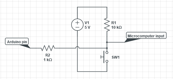
Button circuit with Arduino connection

And the function to control the pins looks like this:

void pulsePin(uint_fast8_t pin) {
  if (pin != pin_invalid) {
    pinMode(pin, OUTPUT);
    delay(pin_mark_time);
    pinMode(pin, INPUT);
  }
}

The pin is driven low for pin_mark_time then tristated. The value of pin_mark_time (in milliseconds) can be found by experimentation. In this case, 100ms worked fine.

The Arduino microcontroller can now control the tape deck, but the remote control still needs to be added.

Infrared remote interface

For the remote control, six redundant buttons on the hi-fi amplifier remote (originally for a CD player which I don't have) which roughly correspond to the six buttons on the cassette deck shall be used.

Remote control buttons

A standard 38kHz IR remote control receiver module is hooked up to an oscilloscope and the waveform is examined to determine the protocol. In the image below, the "Play" button is pressed. The waveform is compared to the example waveforms for various popular remote control protocols that are available online.

RC-5 waveform

The protocol turns out to be the very popular RC-5 protocol and five of the six buttons correspond to the standard RC-5 commands for CD players:

  • Reverse: 33
  • Forward: 32
  • Stop: 54
  • Play: 53
  • Pause: 40
  • Sound Mode: 130

The popularity of the Arduino system means an open-source library is available for almost any IR protocol, so a simple RC-5 library is selected for this project. The library is licensed under the permissive 2-clause BSD license. The included code example which prints received codes via the UART confirms the command codes listed above, so all that's left is to pulse the output pins when the appropriate code is received.

In addition to the command code, the RC-5 packet also includes an address, which the library decodes as well. The address allows multiple devices of different types to use the RC-5 protocol without interference. Unsurprisingly, it's the standard CD player address (system 20).

Putting it all together

The full code for the Arduino-based IR cassette deck controller is on my GitHub along with some comments which explain how the code works.

All that remains is to transfer the design to some permanent hardware. I chose to build the final version of the design directly on stripboard instead of using an Arduino plus a shield to make the solution more compact and make it easier to integrate it into the equipment.

An ATmega328p with the Arduino bootloader is used. It could be ported to a smaller microcontroller to make it even more compact, but I didn't perceive the effort as being worth it for this one-off case, so I stuck with the ATmega328p. The necessary components are soldered to the stripboard along with wires to connect it to the "microcomputer PCB" of the cassette deck. The buttons all share a single connector, so the soldering is neat and tidy here. Power is also taken from the microcomputer PCB. The stripboard assembly is mounted on a convenient ledge using hot glue.

Close-up view of the stripboard assembly
View of the inside of the Yamaha K-220 cassette deck with the infrared remote control mod added

Finally, the infrared sensor needs to be placed somewhere. As the cassette deck was not originally designed for a remote control, there is no official place on the front panel for it, but through careful positioning, it is possible to install it without needing to cut any holes without significantly compromising the IR sensitivity.

The IR sensor is installed behind this knob. Whilst refitting the knob does affect the sensitivity somewhat, the sensitivity is still good.

Knob removed showing the position of the IR receiver
Knob refitted, hiding the IR sensor

Saturday, July 11, 2020

VHDL Teletext Decoder Part 3: Data recovery, processing and page extraction

In Part 2, I designed a display controller which can display a 40 character by 25 line screen of text and graphics as used by Teletext (and Mode 7 on the BBC Micro). The display controller reads from a dual-port RAM, which means it can be used in any FPGA project where data display and basic graphics are required. In the case of a teletext decoder, the VBI data needs to be extracted from the composite video signal, error correction needs to be applied, and then the data relating to the currently selected page number needs to be loaded into the dual-port RAM so that it is displayed by the display controller.

RTL block diagram

The teletext decoder section of the design has been broken up into four modules:

  • TXT_DATA_RECOVERY: Detects the start of a packet (line) of teletext data and extracts the serial data
  • TXT_DESERIALISER: Converts the serial data to parallel
  • TXT_DATA_PROCESSOR: Performs error correction on the data and determines the page number and subcode of each packet received
  • TXT_MEMORY_CONTROLLER: Writes packets from the selected page number to the dual-port RAM

Parallel vs serial transmission schemes

Not to be confused with serial and parallel data, these terms refer to the order in which pages are transmitted in the VBI (Vertical Blanking Interval).

In a parallel mode scheme, a few lines from one page in a particular magazine are transmitted followed by a few lines from a page from another magazine and so on. This approach was favoured by UK broadcasters when teletext was broadcast here and is still used by TEEFAX. This scheme can be identified from the display of page numbers only from the current magazine in the rolling header when waiting for a page.

In a serial mode scheme, all packets transmitted belong to the page number and magazine of the last header packet transmitted. This approach is favoured by international broadcasters, and is identified by page numbers from every magazine being displayed in the rolling header.

More detailed information about these schemes is described in Annex B of ETSI EN 300 706.

TXT_DATA_RECOVERY

This module detects the start sequence of the packet then forwards the serial data onto the next module. The start of the packet is shown below:

To simplify the design and avoid the need for a high-speed ADC, the packet is simply digitally sampled, which means the module only has a single digital input. A high-speed comparator is the only active semiconductor required, although the user may have to adjust the trimmer pot RV1 when switching sources.

Composite video input and sampling circuit

The comparator converts the analogue signal into a digital signal suitable for the FPGA:

The data recovery module, along with the rest of the teletext decoder section, runs at 27.750MHz, four times the data bit rate. A SI5351 programmable clock source is used to generate this unusual frequency with great accuracy along with the unique video clock required by the VGA controller for each resolution.

There are four sampled bits per data bit (known as 4x oversampling), and the bit rate has a very tight tolerance so there is no need to worry about clock recovery, which simplifies the design a lot. A shift register is continuously fed with the digital data provided by the comparator and a packet is detected once the start sequence is detected in the shift register. One out of every four bits will be sampled during the inter-bit transition, so the comparison is performed using only three sampled bits in every data bit, then the data sent to the next module is recovered from the middle sampled bit of each subsequent data bit.

Start pattern in teletext waveform

The colour burst is not sampled, nor is the video line number counted. These are not necessary for decoding, and the only consequence is the decoder will be capable of receiving anything transmitted otherwise in accordance with the specification which may be rejected by a commercial decoder.

TXT_DESERIALISER

This module converts the recovered data from serial to parallel. The FRAME_VALID_OUT signal indicates the start and end of each packet received to the next module.

TXT_DATA_PROCESSOR

This is the most complex module in the teletext decoder.

Page number detection

The two main types of packet are page header and normal packets. There's also non-displayable packets, but those will be explained later.

Teletext packet types

Every packet contains the magazine number, which is the leftmost digit of the three-digit page number, however, only the header packet contains the remaining two digits of the page number and the subcode. When a parallel transmission scheme is used, pages from different magazines may be transmitted on different lines in the same video frame, which means that the data processor must remember the page number and subcode of the last transmitted header packet for each of the 8 magazines. This is stored in the PAGE_AND_SUBCODE_CACHE whenever a header packet is received and retrieved whenever a packet other than a header packet is received so that the correct page and subcode is always sent to the next module along with the decoded data.

Packet processing

Hamming coding is used to protect certain data such as the page number and subcode to improve the chances of the header packet being decoded correctly in cases of poor reception. This reduces the chance of an incorrect page being loaded on top of the displayed page when a subsequent header packet is incorrectly determined to have the selected page number. Unfortunately, Hamming code dramatically increases the number of bits taken up by each piece of data, so it is only possible to use it for the most important data, and the display data is only protected with a simple parity check with no error correction capability because it is less critical that every display byte is correctly decoded. It should be noted that correct decoding of every single display byte is expected when the signal quality is good and there is no interference.

The parity checking and Hamming decoding is carried out by sub-modules (VHDL components) in TXT_DATA_PROCESSOR.

TXT_MEMORY_CONTROLLER

This module selects the appropriate address in the dual-port RAM to write each packet belonging to the specified page number to, then forwards the packet data on to the dual-port RAM.

It also controls the display of the status line. The last 8 characters should be continuously updated regardless of the magazine of the header row, whilst the rest of the header row should only be updated when waiting for a newly-selected page number ("search mode"), in which case only header rows from the current magazine should be displayed when the pages are transmitted using the parallel transmission mode, and header rows from all magazines should be displayed when pages are transmitted using the serial transmission mode.

This module also extracts the editorial links (also known as Fastext) for the four coloured buttons and the index button from the relevant non-displayable packet.

The 8 characters in the top left corner of the display are called the status characters. These are controlled by the keypad controller, and are used to display the page number and subcode number. The memory controller monitors these characters and updates the dual-port RAM whenever they change. The UPCOMING_FRAME_IN signal ensures that page content updates (which must happen in real-time) are prioritised over updates to the status characters.

The REQ_SUBCODE_SPEC_IN signal is set when the user requires a specific sub-page to be displayed. When the Time-Text button is pressed, the keypad controller sets the REQ_SUBCODE_SPEC_IN signal and the memory controller will then only display pages where both the page number and subpage match the requested values, otherwise the subpage is ignored and all subpages from the current page will be displayed as they are received.

Screenshot of the project in operation

The project can decode pages generated by VBIT2 running on a Raspberry Pi.

Teletext decoder connected to a display, showing a teletext page

Next: Data recovery, processing and page extraction

Saturday, April 18, 2020

VHDL Teletext Decoder Part 2: Page Display including Text and Graphics

In Part 1, I designed a very simple VGA controller, but without any content to display, it's not very useful. The next part that's required is the display controller, which is responsible for drawing the text, graphics and colours on the display.

The Display Controller shall take its input from the read side of a dual port RAM, which shall be written to by the Teletext Data Processor in this project, but the Teletext Data Processor could easily be replaced with something else for non-Teletext applications. A Display Controller based on the Teletext specification makes an excellent FPGA display generator, even for non-Teletext applications. This is because the specification was designed in the 1970s to be relatively easy to design an ASIC around, which means that the compiled logic size is very small compared to modern FPGAs, and makes it very "cheap" in terms of resources to add the display generator to any project.

This is generated entirely by an FPGA

Level 1 Teletext supports text and graphics via a character generator ROM, mosaics of 2x3 pixels, and selectable background colour.

Key display features

Text

The font used was taken from the datasheet for the Texas Instruments SN74S262N CGROM, originally used in the 1970s "Tifax" decoder design, and entered into a VHDL file.

The CGROM has a row output format, which is better than column output for horizontal-scanning display systems because the input address only has to change once for each character along the line currently being drawn rather than for every pixel.

Graphics

Basic graphics capability is provided by 2x3 mosaic tiles:

Careful examination of the mosaics set will reveal that each of the six tiles in the mosaic correspond to particular bits of the address. No additional CGROM is required, and the logic to draw the mosaics ends up being very simple. The addresses marked (1) are displayed from the CGROM; this allows CAPITAL LETTERS to be mixed in with mosaic graphics without having to switch between text and mosaic modes.

Mosaics can be contiguous or separated; this is set using spacing attributes.

Double height text

Double height display can be enabled at any point on a line, and applies to any characters or mosaics drawn after the Double Height command up until the end of the line or a Normal Height command. If a Double Height command is used anywhere on a line, the entire line below is ignored (even below characters that aren't double height), which seems strange, but this simplifies the logic design. The CGROM glyphs are easily "doubled in height" by bit-shifting the row selector right by one bit when in double height mode, with just a little bit of extra logic required to correctly draw the second line.

Colours

The available colours are: White, Yellow, Cyan, Green, Magenta, Red, Blue, Black. All of these can be output using only one bit per channel (R, G, B). Black cannot be used as the foreground colour in standards-compliant Level 1.0 and Level 1.5 Teletext decoders, but most modern decoders will interpret it anyway. Not interpreting it does not make the logic simpler, but my decoder will be designed to not interpret it in order to stick as closely to the specification as possible.

Spacing attributes

All attributes are set using these commands. They are called "spacing attributes" because each one takes up a space on the display. Level 2.5 and 3.5 Teletext also supports non-spacing attributes which do not take up space on the display, but that is outside of the current scope for this project.

All attributes are described in detail in Section 12.2 of the ETSI EN 300 706 V1.2.1 Enhanced Teletext Specification.

Attributes can be "set-at", meaning they apply immediately, or "set-after", meaning they apply from the next character position onwards. Correct implementation is required to ensure the correct display of "held" mosaics. Hold mosaics is a feature which displays spacing attributes as a repeat of the last mosaic to enable seamless colour changes; without hold mosaics, spacing attributes would always be displayed as spaces and graphics like the famous Ceefax weather map would not be possible.

Mix and Reveal

The Conceal attribute hides text and mosaics. Setting the Reveal input high will display the hidden content.

The Mix feature on a real TV displays the foreground content on top of the TV picture. All background colours effectively become transparent. Currently, the design has no capability of drawing the text on top of an existing video signal, so all this function does at the moment is show all background colours as black. The Start Box and End Box attributes are unimplemented for the same reasons.

Firmware

The main parts of the logic are:

  • Combinational logic for mosaic generation
  • CGROM
  • Active area controller: Determines whether we're currently in the area of the screen where the content will be drawn using a set of constants which determine character height, display height and width, characters per line, and number of VGA pixels per Teletext pixel
  • Line and character counters: each pixel and each row within each character needs to be counted
  • Display generator: reads the dual port RAM data and interprets the spacing attributes
  • Logic to control setting the output signals to the foreground/background colours, and flashing

Teletext uses 40 characters and 25 lines, but the display controller is in no way constrained to that, and this can easily be changed using constants in the code for other applications.

Development

As the Display Controller operates independently of the Teletext decoding, development can be done without the decoder by loading a Teletext page into the dual port RAM by specifing it as the default data in Quartus. It is not possible to use .tti files directly because the spacing attributes are converted into ASCII sequences, and unnecessary header stuff is added, but it's simple enough to convert it to raw data by hand.

Here's the display from an early version of the display decoder:

A largely-completed display generator combined with working teletext decoder:

The firmware is available on GitHub

Despite making little attempt to "optimise" the code, the whole system including teletext decoding takes up only 6% of the small (to modern standards) 22k logic element Cyclone 10 LP FPGA.

Still to come...

Next: Data recovery, processing and page extraction

See all posts with the label Teletext to see my future progress on this project.

An additional challenge would be to design firmware to synchronise to an external VGA signal and draw text on top of the incoming VGA signal.

Wednesday, April 15, 2020

Driving a VGA monitor from an FPGA made simple (VHDL Teletext Decoder Part 1)

When your FPGA project needs to display a large amount of data, there is one solution which is simple but may not be obvious: the VGA monitor. An analogue monitor from a digital FPGA, really? Yes, it's actually really straight forward to generate VGA signals, and no external chips are required to do so. This topic has been covered many times before by others, and in this blog entry I will try to simplify it as much as possible whilst including some important details that are sometimes missed. HDMI/DVI are covered later in the series...

Project objective

If you haven't read it already, please read the introduction to the VHDL Teletext project over on my dedicated VHDL Teletext Overview blog entry, which covers the project objectives, a brief history of Teletext and its current uses, and the FPGA Teletext hardware.

The basics

The hardware

VGA has five key signals - R, G, B, Horizontal Sync, and Vertical Sync. There are additional signals which can be used to get details of the monitor via I2C, but those are outside of the scope of this entry.

Horizontal Sync and Vertical Sync are TTL-level digital signals, but it is sufficient to use 3.3V FPGA pins directly. These are not terminated in the monitor, so you can use low value series resistors to protect the FPGA pins in case of a short circuit without affecting functionality.

R, G and B are the analogue signals, which are terminated with 75 ohms inside the monitor. 0V corresponds to black and 0.7V is full brightness. A simple resistor ladder DAC will suit most FPGA applications; the design is very simple: decide how many "bits" of colour depth are required, then calculate the resistor values so that they follow these rules

  1. The voltage at the output, when terminated with 75 ohms, is approximately 0.7V when all FPGA outputs are on
  2. Each bit in order of decreasing significance should have a resistor value of double that used for the last bit

For many text-based applications, all that is required is one bit per channel, in which case a 270 ohm resistor is ideal when using an FPGA IO voltage of 3.3V.

The firmware

The firmware is simple too; there's just a few terms which need to be understood, and the best way to explain these is with a diagram:

The dotted arrows indicate the retrace of the electron beam on CRTs; this happens during the blanking interval. LCDs don't have a retracing anything, but the timings remain the same for compatibility. The scanning is done from left to right, top to bottom. The HSync waveform happens once per line, whereas the VSync waveform happens once per frame, so the HSync signal will pulse hundreds of times for each VSync pulse.

Translating this to HDL, all that's needed is:

  1. A "Horizontal" counter which is normally incremented once per clock cycle
  2. A "Vertical" counter which is incremented every time the Horizontal counter completes a full cycle
  3. Some logic to generate the sync signals and ensure the video is blanked during the blanking intervals

But wait...

VGA was originally designed for CRT monitors, but nowadays it is frequently used on LCD monitors. How does it know what the horizontal time period of each pixel is when it doesn't know what the pixel clock is?

Well, it doesn't. The "Auto Adjust" function attempts to work this out, but it only works if the active area is full of content. If you're using a black background and the content doesn't reach the edges, then the Auto Adjust function may not work correctly. To ensure correct Auto Adjustment when using a black background, a border around the edge of the active area should be drawn. This will, of course, be visible on the monitor, but that's only a minor price to pay to guarantee correct adjustment. This is easy to implement with a line of combinational logic.

Resolution selection

The resolution is limited by the speed of the FPGA, the quality of your hardware, and the length of your cables. The resolution is normally dictated by the requirements for what needs to be displayed.

The most common resolution is 640x480; with a pixel clock of 25.15 MHz, this can be closely matched using a common 25MHz clock. 1280x960 can be achieved with a 100MHz clock. High resolutions can be achieved with lower clocks if you are happy to use non-square pixels (wider than they are tall).

It's a good idea to specify the parameters using constants or generics to allow them to be changed easily. Any experimentation should be done with an LCD monitor, since some CRTs can be blown up by improper timings. Here are some typical timings for 640x480:

  • H Size: 640 clock cycles
  • H Front Porch: 16 clock cycles
  • H Sync Pulse: 96 clock cycles
  • H Back Porch: 48 clock cycles
  • V Size: 480 lines
  • V Front Porch: 11 lines
  • V Sync Pulse: 2 lines
  • V Back Porch: 31 lines

The calculation for the required clock frequency is: F (Hz) = Frames per second * (H Size + H Front Porch + H Sync Pulse + H Back Porch) * (V Size + V Front Porch + V Sync Pulse + V Back Porch)

For most monitors, the frames per second should be around 60Hz. The lower limit is usually around 50Hz, and the upper limit 65Hz, or 80Hz for most monitors with a resolution of 1280x1024.

Example code

Link to my example code (read the points below first)

  • My code just outputs internal sync signals, but you may desire to output the pixel counter values instead; this would be simple to implement. (hint: convert integer to std_logic_vector)
  • This code does not generate any display content on its own, not even the test card. Generating this is a challenge for the reader.
  • The timings have been modified for 720x576 resolution, therefore the clock frequency required is higher (see equation above). The border generator has also been written to draw the vertical borders offset from the edges. LCD monitors which can't sync to this resolution should detect it as 800x600.

Next: let's generate our content.

Sunday, March 15, 2020

Why does the cycle life of EEPROM and Flash need to be considered in your design?

Most microcontrollers nowadays come with up to a few kilobytes of EEPROM, and this memory is frequently used to store user settings and sometimes for basic logging. Flash-based microcontrollers have EEPROM because Flash memory must be erased in large blocks (pages) before writing, which is fine for program memory, but inconvenient for settings where only a few bytes need to be changed and storing a whole page in RAM to re-write may be inconvenient.

Here's the parameters for the various types of memory in a popular microcontroller:

One thing you may be quick to forget about is the number of write/erase cycles. "100,000 cycles, that's a big number, great, don't need to worry about it."

That is a bad approach. Cycle life is important; especially if you don't want your company to gain a reputation for making "landfill electronics", "lagdroid phones", or "cars that frequently need expensive electrical repairs out of warranty..."

I'm not going to demonstrate using a program which repeatedly writes the same location for ever more; I will focus on practical examples.

A practical demonstration

This is the Dashboard Display 1.0:

Using a GPS module, it measures the current speed, and the distance and time taken for each trip. I'll cover the project in more detail later. It's also the forerunner to the much more advanced project I did for my university dissertation, Global Positioning System and European On-Board Diagnostics-based Automotive Monitoring System.

The Dashboard Display was designed to be continuously powered, with connection to the vehicle via a short car radio extension cable with spliced-in cables running to the multi-pin connector on the front. These connections allowed the backlight to automatically come on and dim when required. The trip distance and time were stored in EEPROM just in case the power was disconnected, however.

The power was disconnected after six months, and this is what came up when power was restored:

How did that happen? My first guess was that I had made a type casting error in C, but that error usually results in losing 1s off the left of a variable, not gaining them. Additionally, the problem came back after resetting the trip counter and cycling the power again.

I examined my code and found that it saved the time and distance to EEPROM once a second, even when the trip counter was not running (it paused itself whenever no movement was detected). As a result, the same eight EEPROM locations were written around 15000000 times, or 150 times the maximum rating. I wrote a little test program to test it, and these 8 locations were well and truly banjaxed, being unable to hold the freshly written data for even the few microseconds it took for my program to read back the values.

All 8 bytes were affected, since the microcontroller cannot erase individual bits, and does not have the intelligence to not erase unchanged bytes unless programmed to check them. Interestingly, the bytes still passed testing when a sequence of 11111111 was written, and only failed when patterns of alternating bits were written, suggesting that neighbouring bits influence failing bits. The failing bits were always read back as 0 when alternating bit sequences were written.

Where was the mistake made?

It's easy to put the blame on the piece of code which was supposed to not write the trip values when the trip counter was paused but didn't, but that's the wrong attitude. It's true that the EEPROM would have suffered much less wear had that mistake not been made, and it would have taken a much longer time for any problems to surface, but the mistake was in fact the decision to write the trip data every second. That decision was made to ensure accuracy of the data should power be lost temporarily, with no consideration made for longevity. Had the code been written correctly (according to specification), it would have needed only 27 hours of continous driving to exceed the rated lifespan of the EEPROM. The rated lifespan is usually worst case (highest voltage and temperature), but this should not be acceptable.

The frequency of saving data to EEPROM must be carefully considered when designing a product. In this case, it's unlikely that power would be lost mid-trip, and it would probably be acceptable to save the data only when the trip is stopped or reset, which is how the Global Positioning System and European On-Board Diagnostics-based Automotive Monitoring System handles this problem.

If you really need to write often

With ever increasing flash memory density and cost pressures, the cycle life of flash memory can be as low as 1000 cycles. Wear levelling is a technique used by modern flash-based mass storage and works well as long as there is a good amount of "unused" space. This technique can also be used on a microcontroller, but is not without its challenges.

Other solutions include using FRAM, which is similar to EEPROM except with practically unlimited cycle life, and battery-backed SRAM.

But the best solution is to minimise how often you write data. And if you're writing logging data, do you really need to?

A commercial example

Here's an example of how such a simple oversight can affect even the biggest companies:

Photo by Tokumeigakarinoaoshima - licensed under CC BY-SA

The MCU is the main computer in Tesla cars, and it uses eMMC Flash memory. The software writes a lot of logging data, and this in conjunction with the relatively small 8GB Flash chip results in the Flash getting worn out in just a few years on heavily used cars. The only official repair is replacement of the MCU costing £2500+ out of warranty.

At least in this case, this problem can be mitigated somewhat with software updates. Many embedded projects do not have that luxury.

Learn more about this issue here: https://teslaownersgroup.co.uk/kb/emmc-chip-failure-what-is-it-should-i-be-worried-what-can-i-do

Do you know of any other commercial examples? Let me know in the comments.

Friday, February 21, 2020

Experimenting with a programmable RF Modulator (making a controller for it and testing harmonics)

I was scavenging two old Sky boxes for parts, and although the very large scale integration of the mid-noughties set-top boxes meant there was very little worth removing, I did extract two of these RF modulators.

RF Modulators convert composite video and audio into an analogue TV channel that can be received on any television set and combines it with the signal from the RF input, enabling the picture from the Sky box to be received on every TV set in the house in addition to the off-air channels. Sky RF modulators are unique in that they have two outputs, one of which features line power and a low-frequency return path to support the "digilink" system, which allows the Sky box to be controlled from the other TVs. See diagram of this setup. This blog entry, however, will focus on the RF output rather than those additional features.

The modulator is completely shielded, but the shielding clips off easily to expose the insides. Much like the rest of the Sky box, the modulator is very highly integrated, and it uses a Freescale MC44BS373CA single chip solution. Impressively for a design which handles signals of up to nearly 1GHz, the modulator is built on a single-layer PCB, presumably to keep costs low. The circuit appears to be largely based on the application circuit in the datasheet, with the addition of some passives and transistors to handle the line power injection, IR return path, and amplification of the RF input. The 75-ohm termination resistor on the video input is missing.

The MC44BS373CA is frequency-agile, which means it can be programmed to work at different frequencies, all the way down to 45MHz in fact. Despite this, the Sky box only allows selection of UHF channels, despite VHF System I still being used in Ireland, so let's find out why not...

Programming the modulator

The modulator has a very simple I2C interface documented in Table 8 in the datasheet, and it supports 5V and 3.3V operation, allowing easy interfacing to Arduino, Raspberry Pi, etc.

The controller is supposed to have a programmable I2C address, but this feature is not available on the package used in this modulator, so it is fixed to 0xCA (8-bit).

There's not a lot of settings that can be configured. The main settings of interest are the oscillator frequency (N11:N0), divider (X2:X0), and test pattern enable (TPEN). The sound frequency bits (SFD1:SFD0) should simply be set to the appropriate setting for the region (10 for System I).

The relationship between frequency, divider and N11:N0 is simple, and I've put it into a table here:

X2:X0 (Divider) N11:N0 F (MHz)
000 (1) 4F N/4
001 (2) 8F N/8
010 (4) 16F N/16
011 (8) 32F N/32

The oscillator is rated for 460MHz to 880MHz, so it's necessary to use the divider to use lower frequencies.

Example project

I made an Arduino sketch to control the modulator. It allows selection of the channel number, from which the frequency and divider are automatically calculated, plus selection of the system (B, D, I, M) and the test pattern.

I haven't included a schematic because the wiring is very simple; all pins are defined in the code. The only important components to remember are the pull-ups on the I2C bus (hidden under the LCD) and the 75-ohm termination resistor between Video In and GND. Failure to include the latter results in horrendous close-spaced ghosting caused by signal reflection.

This controller was used to enable easy control of the modulator during testing.

Link to the code on GitHub.

Real-world testing

My current oscilloscope can only show the spectrun of signals up to 25MHz, so we can't look at the output spectrum, but what we can do is examine the output picture under various different test conditions.

The datasheet gives two figures for the minimum frequency in different places: 30MHz and 45MHz. The latter seemed to be true.

The programmable oscillator seemed to work down to about 400MHz, below which there was no output and it was necessary to up the divider. It worked fine up to 900MHz, the highest any TV I had went up to, so it may have gone even higher.

The single-sided board didn't seem to compromise the quality at higher frequencies.

The picture had lots of 'sparklies' when using the highest divider (16). It's not needed to access the lowest frequencies anyway.

Harmonics

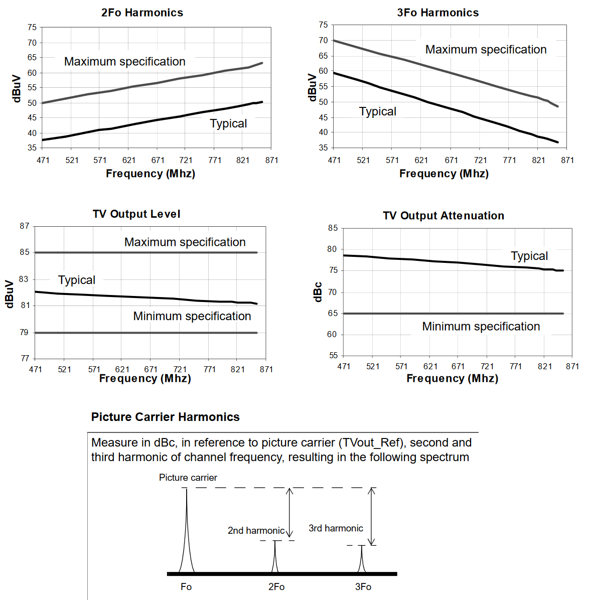
What parts are of particular interest? These graphs...

Look at the signal levels of those harmonics. Unlike this newfangled digital stuff, analogue TV is very suspectible to interference, and a signal to noise ratio of 46dB is required for noise-free viewing. These harmonics result in a signal to noise ratio well below that at affected frequencies, which will spoil anything on those frequencies. The 2nd harmonic is at two times the set frequency, 3rd at three times, and so on, so this isn't a problem when using UHF output frequencies, but at VHF output frequencies, this becomes a problem.

Example 1: Set frequency (1st harmonic) 119MHz, harmonics at 357MHz, 595MHz, 833MHz.

Example 2: Set frequency (1st harmonic) 48MHz, harmonics at 144MHz, 240MHz, 336MHz, 432MHz, 528MHz, 624MHz, 720MHz, 816MHz.

Here we examine the harmonics on a TV screen when the test pattern is enabled. The datasheet only shows graphs for the 2nd and 3rd harmonics, but in fact there's a lot more where those came from; whilst I couldn't find the 4th harmonic, the 5th, 7th, 9th, and so on, are quite strong too, but each harmonic is weaker than the last.

Now let's see what happens when one of those harmonics happens to correspond to a TV channel. An analogue channel is viewed on C24 (495.25MHz), and the modulator is set to 165.08MHz (then 99.05MHz) so that the third harmonic (fifth harmonic) is at the same frequency as the channel being viewed. Note that the Arduino example cannot select this frequency, so a direct I2C write is required (N=2641, divider=4).

Unsurprisingly, the result is terrible co-channel interference, which looks like this:

When the third harmonic is the source of the interference, it is possible to see a faint image of the picture being transmitted by the programmable modulator. The interference is reduced with higher harmonics. The last screenshot shows the quality of the 5th harmonic with the source of the real C24 disconnected.

Noise of a different kind

The convenient 5V power supply makes it tempting to power projects using it from a phone charger. This should be done with great care, as any noise from the power supply will be visible on the modulated output. I can't provide a screenshot of this; the picture has to be watched to understand the irritation of the effect properly.

Summary

These modulators provide good results and flexibility as long as their limitations are considered. The I2C interface allows easy programming and integration into video-based microcontroller projects such as VBIT-Pi (as long as the noise is considered), and the loopthrough and dual outputs allow easy integration into TV distribution systems. The only real limitation is that when VHF channels are used, it will usually be necessary to use external output filters to combine the new channel with a distributon system to avoid interference from the harmonics.

Other bonuses of this modulator include the high signal output level, which allows the signal to be split to many TVs without introducing noise, plus I believe the RF input is amplified a bit too, though I haven't been able to test that.

Tuesday, January 28, 2020

6-inch jumbo radio-controlled LED clock/timer

Large radio-controlled 7-segment blue LED clock

First completed: 2013

This was my A2 Level Electronics project, and the objective of this project was to create a clock/timer/stopwatch for a big hall which was large and bright enough to be clearly visible from across the hall. It also needed to synchronise the time automatically, like a radio-controlled clock.

Emphasis was placed on support electronics in my design because it was undesireable for A2 Electronics projects to focus too much on software.

Power supply selection

As good power efficiency over a wide range of operating voltages was desireable, an efficient regulator was required.

A linear regulator such as the 7805 simply turns "excess" voltage into heat, so if the LEDs required 5V, and the power supply was 20V, the regulator would only be 25% efficient. A switching regulator uses an inductor to efficiently step the voltage down with low losses. The MC34063 switching regulator was selected to ultimately power the LEDs because of its low cost, good availability, and 500mA current rating, which was adequate for the task.

The MC34063 is a rather old switching regulator operating at a low frequency compared to modern ones, but it was fine for this application and it was still a lot more efficient than a linear regulator. The low frequency also meant that the layout of the circuit had little effect on the performance of the switcher.

I tested the efficiency of this regulator with two different supply voltages. Despite the stripboard construction, the efficiency figures were not far off that in the datasheet. 2020 note: Constructing a modern high-frequency switcher this way will totally decimate its performance, based on the author's experience.

Switching regulator efficiency
Switching regulator on stripboard

Microcontroller architecture

This was one of the author's first Arduino projects and very ambitious for the author's skill level at the time, so the design was simplified a little by delegating the task of decoding the radio-controlled time signal to a PICAXE microcontroller. PICAXE was the first ever microcontroller system used by the author - it is a family of pre-programmed PICs running a special BASIC interpreter and aimed at the educational market; it's too slow to handle all functions of the project, but its key feature of being very easy to configure as an I2C slave made it a perfect fit for the task of handling the radio controlled time decoding. The ATmega328p microcontroller handled almost everything else, except the timekeeping, which was delegated to a DS1307 RTC and backed with a coin cell to allow immediate display of the (roughly) correct time on power-on.

System block diagram

At the time, the author was new to the Arduino/AVR platform, so some of the handy features of the platform, like interrupts, were neglected. The C program runs in a big loop: checking the buttons, performing I2C bus operations, and lighting up each of the six digits one at a time. This was not a real problem though, as the Arduino libraries provided handy functions like millis() to help with timing and there weren't any operations that took a long time to execute.

Radio controlled time (MSF / Time from NPL) signals on oscilloscope

The PICAXE decodes the Time from NPL using the bit-bang method and places it into "scratchpad" (a large block of memory inside the PICAXE that can be read by the I2C Master); the signal was essentially a serial signal with a baud rate of 10. The demodulation from 60kHz was done using a commercial off-the-shelf receiver.

Hardware development

The first prototype was built on breadboard using small 7-segment displays along with an additional microcontroller programmed to simulate the output signal from the radio controlled time receiver; the signal is susceptible to noise, making development using the real receiver difficult.

Prototype of the radio-controlled clock built on breadboard

The circuit was then built up on stripboard to make it permanent along with the addition of the transistors required to drive the big displays, which would be added later. A brightness selector switch was implemented by switching a second trimpot in parallel with the switching regulator's feedback resistor. This board was initially tested with small displays.

Control electronics built on stripboard undergoing testing

The display was made from a sheet of acrylic cut on the laser cutter. All 408 LEDs were pushed in and soldered by hand.

LEDs being pushed into the sheet of acrylic

The stripboard assembly was attached to the back of the display.

Picture of the stripboard assembly mounted on the back of the display with all major parts labelled

Summary

The project met its design goals; all intended functionality (clock, stopwatch, countdown timer and radio controlled synchronisation) were implemented and worked, and the display was bright and readable even outside.

Picture of the big clock outside

The power consumption of the display was tested over a wide range of supply voltages. The maximum power consumption with all segments on was 4W.

The code is available on GitHub. The code is extensively commented, but as one of my first Arduino projects, it's far from a shining example of C programming.

Large dot matrix clock, timer and scrolling message display

First completed: August 2014. Additional work carried out late 2025/early 2026. Introduction Previously, the author had made a very small ...