Sunday, July 11, 2021

Animated dot matrix display radio-controlled clock

First completed: May 2013

Small dot matrix display hardware

Introduction

This project was my first attempt at driving a dot-matrix LED display from a microcontroller without using any dedicated driver chips. It was also, at the time, my most advanced PCB design. Prior to this project, the most complex LED multiplexing I had done directly from a microcontroller was a 6-digit 7-segment display, which in terms of complexity is equivalent to a single 8x6 LED dot matrix.

I decided to use an ATmega328p pre-programmed with the Arduino bootloader for this project.

Hardware

The main elements of the design are the microcontroller with its supporting components, the displays with their shift registers (these are hidden behind the displays on the PCB), and a switching regulator.

The schematic below shows the design excluding the switching regulator.

Schematic

The shift registers are a serial-in-parallel-out type, and were needed because the ATmega328p does not have enough pins to drive the display directly. The shift registers are 74HC164, as with the Noughts and Crosses game.

The PCB layout was done by me, but the board itself was made by a third party. The PCB was made on a PCB router and the board is not through-hole plated - I learned a very important lesson here as to why through-hole plating is usually important. The design relied on through-hole connections being connected to both sides, so it was necessary to solder some of the pins on both sides to simulate through-hole plating.

Software

The LED displays are multiplexed. Only one row of the display is lit at a time; each row is switched on in turn very rapidly, and this technique relies on persistence of vision to make it look like the entire display is continuously lit.

The animation below shows the technique in action but for column scanning.

Multiplexing animation

Initially, the software was a simple design which just used delays in the main loop of the code to switch between the rows. This method works reasonably well on the ATmega328p at 16MHz because it can execute instructions fast enough to avoid functions in the main code from having a visible effect on the display, but it makes writing the code more difficult because delays and "slow" commands cannot be used. The software design was later enhanced by using a timer interrupt to run the display software, making its timing independent of what happens in the main code.

The display shows the time, and a scrolling effect is used whenever a digit changes. The time is synchronised using a "Time from NPL" receiver, the signal from which is decoded by the software. The use of the timer interrupt for driving the display, the author's extra experience with using the ATmega328p, and the removal of the external RTC allowed the time decoding to be done without the extra microcontroller that was used in the 6-inch jumbo radio-controlled LED clock/timer project.

Saturday, March 20, 2021

Noughts and Crosses Game

First completed: 2011

Introduction

This is a simple electronic game that I made as part of my Art & Design GCSE at school back in 2010/11. The Art & Design GCSE allows creations made from non-traditional materials, and they can even be electronic, as long as they are arty in some way. This project was inspired by Damien Hirst's spot paintings, and uses LEDs to illuminate each of the "spots" a different colour to represent each player.

Pressing the New Game button will start the game. The colour of the player who goes first is random. The game is purely multiplayer and has no AI. Each player takes it in turns to select their spots, and the game ends once the board is full or there are three spots of the same colour in a row.

Construction

The game is constructed on a single-layer board made on the school's simple PCB production facilities - the board was exposed to UV, etched in a tank, and hand-drilled by myself. The front panel is made out of thick card, and the filling is made from foam which has been cut to shape. The buttons are made from stack of different sized cardboard rings which have been glued together so that they can move enough to press the buttons on the PCB but are retained by the front panel. A sheet of tracing paper covers the front and enables the LEDs to produce evenly-coloured spots when lit.

Picture of the Noughts and Crosses Game
Front view of the buttons
Side view of the buttons

Electronics

The game uses a PICAXE-18M2 microcontroller, which is a PIC microcontroller pre-programmed with a BASIC interpreter specifically for the educational market. As a result, it's slow, but it's fine for this application. The 3.5mm jack is used to program the PICAXE microcontroller using a serial cable.

The other DIP ICs on the PCB are serial-to-parallel shift registers which are responsible for driving the LEDs. The only multiplexed part of the design is the matrix keypad. Note that with more programming skill (and probably a faster microcontroller than the PICAXE), the LEDs could have been multiplexed as well, eliminating the need for the external shift registers, but the PICAXE is missing more advanced microcontroller features like timer interrupts (except on larger devices), which would have made multiplexing the LEDs more complex.

A simple 5V linear regulator is used to supply power to the microcontroller from the user's choice of a 9V battery or external DC power supply.

The PCB was originally designed to use 4-pin buttons throughout, but the buttons needed to be substituted with 2-pin buttons so some jumper wires had to be added.

Front view of the PCB
Rear view of the PCB

Tuesday, January 5, 2021

VHDL Teletext: Overview of the project and the FPGA Teletext hardware

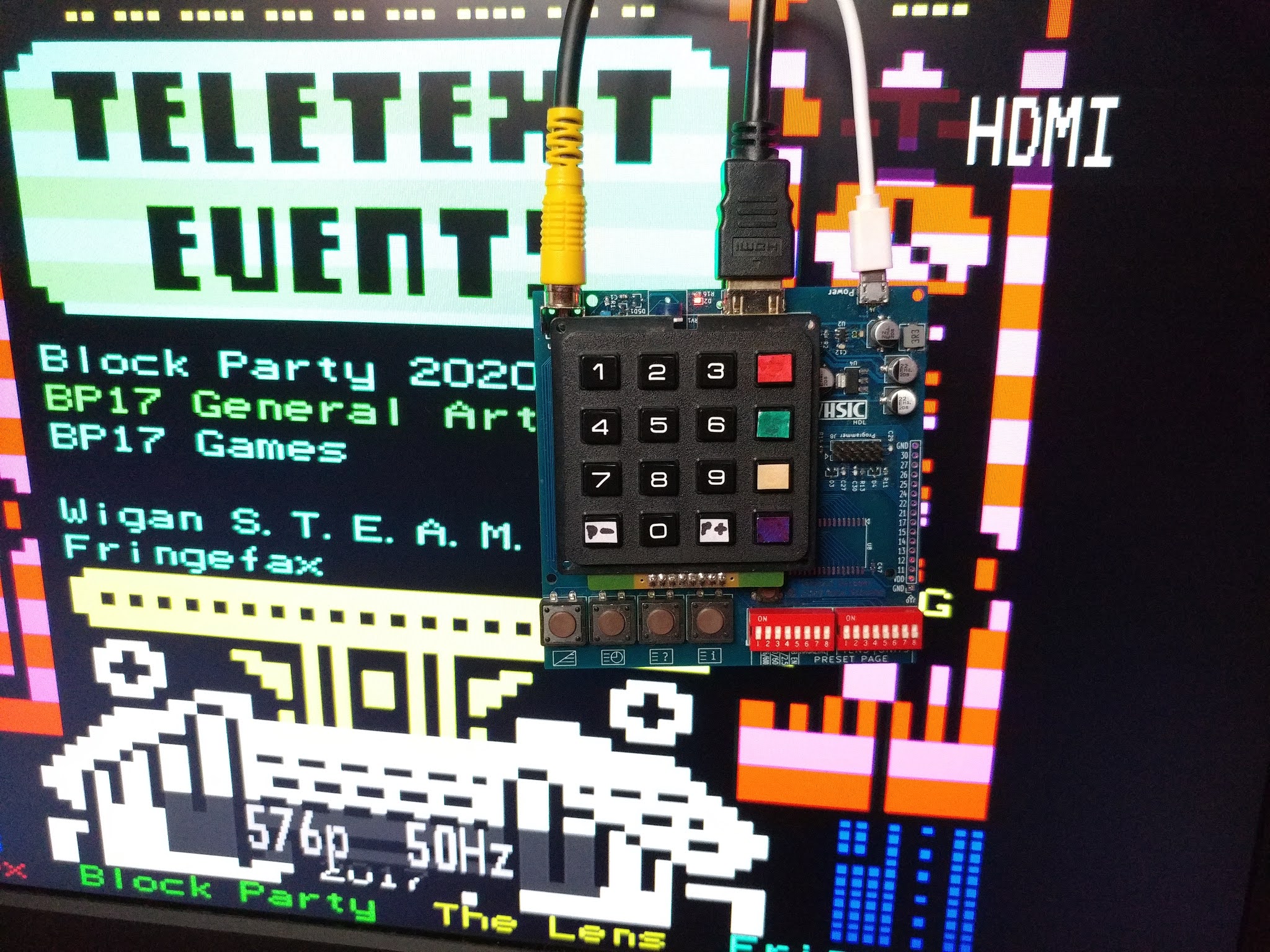
Photo of the FPGA Teletext board in action

Project objective

The aim of this project was to build a fully-featured Teletext decoder using an FPGA. The open-source firmware was written in VHDL. The completed device is the world's first standalone Teletext decoder with an HDMI output, but initially,I implemented a VGA output to learn the basics of generating video from an FPGA.

A brief introduction to Teletext

Teletext was introduced in Europe in 1970s as a system to display text and simple graphics on television sets. A signal contained within the Vertical Blanking Interval (VBI) (of the composite video signal) is decoded by (typically) a custom ASIC in the TV set, which displays the page requested by the user when it is received. World System Teletext (WST) became very popular in Europe and remains in use today (2021) in countries including Germany, Italy, and Ireland. Teletext was also launched in the United States, where it was much less successful, and didn't last very long.

Teletext most commonly carried information for human use such as news, but in the past it also carried programs for computers to use - called Telesoftware.

In the 1990s, Level 2.5 teletext was introduced. It allows Teletext artists to use more colours and more complex graphics. Level 2.5 is not widely supported by television sets, but VHDL Teletext will include some Level 2.5 decoding ability.

Teletext survives despite the switchover from analogue to digital television; the data originally carried in the Vertical Blanking Interval of the analogue picture is now carried as part of the DVB-S signal, and is encoded into the composite video output of most satellite receivers when tuned to an appropriate channel.

Outside of broadcast, Teletext is used as an art form. The Teletext signals can be generated by a Raspberry Pi using vbit2. TEEFAX, started by Peter Kwan in 2016, is one such service that can be run from a Raspberry Pi.

Development process

I've documented key parts of the project development process in detail in my blog:

  1. Driving a VGA monitor from an FPGA - I gained an understanding of the basics of FPGA video generation by displaying simple test patterns on a VGA monitor.
  2. Page display including Text and Graphics - A basic implementation of the Teletext display generator, incorporating most Level 1 features and using RAM pre-loaded with a fixed page for testing purposes.
  3. Data recovery, processing and page extraction - Created the logic for recovering the data from the composite video signal, identifying packets belonging to the requested page, and writing them to dual-port RAM.
  4. A sidestep post - programming the FPGA using a MAX 10 FPGA - The FPGA Teletext board (details of the board are below in this blog entry) can be programmed using a Raspberry Pi, offering an alternative to those who do not have or wish to procure a USB Blaster. The Raspberry Pi is a popular generator of Teletext signals, so it is incredibly useful to be able to reprogram the FPGA using it.
  5. Generating a high resolution HDMI/DVI output from an FPGA using Double Data Rate I/O - Added the logic to produce HDMI signals at resolutions up to 1280x720.

VHDL-Teletext firmware features

  • Open-source firmware GitHub
  • Level 1.0 teletext decoder with single-page memory
  • Selected Level 2.5 and Level 3.5 features implemented
  • Resolution selection via DIP switches: 720x576 or 800x600 at 50Hz or 60Hz (1280x720 available via firmware branch, and 640x480 also possible with minor code modifications)
  • Alpha Black enable switch for selecting between adherence to the original specification or compatibility with certain modern teletext services
  • Power-on page number selection via DIP switches
  • Mix function enables/disables the display of background colours (note that this board does not display the video portion of the composite video signal over HDMI)
  • Subpage selection
  • Reveal button displays and hides "concealed" page content
  • Page selection via number keys, up/down buttons, and Fastext keys
  • Level 2.5/3.5 store function for applying enhancements to Level 1.0 pages
  • Parameterised design enables design tweaks without any programming knowledge

The hardware: the FPGA Teletext PCB

An FPGA development board designed for the application of decoding WST (World System Teletext) and displaying it on a HDMI monitor/TV. The board is programmed with my open-source VHDL-Teletext firmware and all that's needed to complete the setup is a micro USB power supply, HDMI or DVI monitor, and a source of teletext data with composite video out such as a Raspberry Pi running VBIT2 or a satellite receiver. 50/60Hz output and choice of 576p and 800x600 resolutions for compatibility with international TVs.

FPGA Teletext PCB

Development board hardware features

  • 10M08SCE144C8 FPGA
  • HDMI output with arbitrary resolution support* with proper current-mode logic level shifter IC
  • Composite video input with high-speed comparator for WST sampling
  • Micro USB power supply connection - typical current when running teletext decoder firmware is 100mA
  • 3.3V 2A switching regulator (plenty of power for external electronics) and 2.5V LDO regulator
  • 3-channel programmable oscillator
  • 16-way DIP switch
  • 20 buttons (including detachable keypad)
  • Three I/O headers with 23 I/O pins
  • Footprint for optional 512K SRAM for development purposes (footprint can alternatively be used as extra I/O)
  • Footprint for optional video processor IC (SAA7113) (this could be used to implement full composite video to HDMI conversion)

* Resolution support tested up to 1280x720. The master branch of the firmware includes support for 720x576 and 800x600 resolutions, and the 720p mode uses the feature/720p branch.

Closeup of FPGA on the FPGA Teletext PCB

The board is suitable for all manner of FPGA projects. The Altera MAX 10 FPGA has 8k logic elements which is enough for complex hobby FPGA projects. In addition to HDMI connectivity and the built-in keypad and buttons, 23 I/O are connected to headers to allow connection to other devices, providing the potential for diverse applications such as a Telesoftware decoder or a replica of an old microcomputer.

Why did you make it?

I made it because I wanted to create a Teletext decoder which does not depend on obsolete components and has a high-quality, modern, video output connection.

The unique combination of hardware features needed made existing FPGA development boards unsuitable. Limited stocks of old obsolete decoder chips are still available but these only have low-quality composite video outputs and usually only work with PAL TVs.

What makes it special?

This is the world's only standalone teletext decoder with HDMI output.

Hardware for sale

I have assembled a small number of boards by hand and they are up for sale below. If there is serious demand for this PCB, then I will consider getting a proper production run done, and I'll offer a self-assembly kit too. Please comment below on my blog if these are of interest.

Click here to buy the VHDL Teletext PCB on Tindie (fully assembled) - ships from the UK (though all pricing is in USD on Tindie) - please remember that this is currently a very low volume product so I cannot achieve the low pricing of high-volume consumer gear.

Also available on eBay for those who would encounter high fees from their bank/card provider for paying in USD on Tindie or who wish to use the eBay Global Shipping Programme - eBay link.

Monday, December 21, 2020

Generating a high resolution HDMI/DVI output from an FPGA using Double Data Rate I/O (VHDL Teletext Decoder Part 5)

Introduction

I've already shown how to add a VGA output to an FPGA, but a HDMI/DVI output is sometimes more useful, as they offer better compatibility with modern displays, and a much higher bit depth (8 bits of colour per channel) is possible without needing to add extra I/O pins for each bit like you would with VGA. I've implemented a HDMI output as part of the VHDL Teletext project, and the main benefit for that project is that the additional colours supported by Level 2.5 teletext can be generated by the FPGA.

HDMI/DVI are very closely related to VGA, the timings are essentially the same, and it is in fact possible to generate VGA and HDMI/DVI from the same internal signals simultaneously. There is very little difference between HDMI and DVI, but DVI is video only, whereas HDMI usually carries audio as well. Generating audio will not be covered in this article, but any HDMI display should be able to accept a signal without audio, so the implementation in this article can be used for both and the only thing that differs is the choice of connector (the electronics are identical). The interface will be referred to as DVI from here on.

How does HDMI/DVI differ from VGA?

DVI is essentially the digital version of VGA. The main features are:

  • Analogue video channels are replaced by TMDS-encoded digital channels
  • Sync pulses are replaced by special codes that never appear in the active video area
  • Timings can be the same as VGA - timings are broadly categorised as "TV timings" and "PC timings"
  • Current-mode signalling is used on the hardware level
  • Data clock is 10 times the pixel clock, so a high clock speed is needed, but I'll address this issue by using Double Data Rate I/O

This diagram explains how the control signals work for a DVI video signal. Notice how the diagram is very similar to the equivalent diagram for a VGA interface.

Diagram showing the control signals for a DVI video signal

"TV timings" vs "PC timings"

Early HDMI TVs usually only support TV timings, and computer monitors and later TVs usually support all timings (computer monitors may not support interlaced timings, but those are outside the scope of this article). Examples of TV timings are 576p (720x576@50Hz), 720p (1280x720@50Hz and 1280x720@60Hz) and 1080p (1920x1080@50Hz and 1920x1080@60Hz) - 720x576@60Hz is not a proper TV timing, and will not be accepted by most older HDMI TVs. Examples of PC timings are 800x600 and 1280x1024, and PC monitors will often accept any clock frequency you make up as long as the refresh rate is within a certain range such as 50Hz to 80Hz. The most common values for the vertical and horizontal front porch, sync, and back porch for your chosen resolution can be found online (e.g. VESA Monitor Timing Standard).

An additional complication that affects TVs is the RGB Range, which can be "Full range" (0 to 255) or "Limited range" (16 to 235). TVs normally use "Limited range", but unless accurate colour is important, this generally doesn't matter for FPGA applications, especially text-only ones. Limited range was originally used for broadcast applications to avoid clipping analogue signals containing overshoots when they are converted to digital, which could introduce artefacts such as ringing if the digital signal is converted back to analogue.

Timings (EDID) can be read from the connected monitor over an I2C connection. The FPGA Teletext board includes the necessary connections to do this, but this hasn't been implemented in the firmware.

The TMDS signal

Digital video data is encoded using a scheme called TMDS (Transition-minimized differential signaling). It is a similar concept to 8B10B encoding, except the goal is to reduce the number of transitions rather than increase them.

The details of the algorithm are contained within the DVI specification, so I won't explain that in great detail. The algorithm is designed to be relatively easy to implement in programmable logic and in ASICs.

Another detail is that current-mode signalling is employed, whereas FPGAs usually have LVDS outputs, which use voltage-mode signalling. A limited selection of FPGAs have CML outputs, but for those which don't, a converter IC such as the PTN3366 can be used. Using LVDS directly will probably work at low resolutions using a short cable, but I wanted to do it properly on the FPGA Teletext PCB, so I used the PTN3366.

The code

The code is made up of these main parts:

  • Port definitions: the input for each channel is 8 bits, but if the input signal uses fewer bits, you can simply duplicate the bits to generate 8 bits for each channel. VHDL Teletext offers the user choice of two resolutions, so a selector input is provided for that. Pixel clock and high-speed clocks (5x pixel clock) are required.
  • Counter: controls the active area and pixels
  • Sync generator: determines whether the HSync, VSync, both, or no sync control codes should be used according to the counter values and resolution selection
  • TMDS encoders: three identical encoders for the three channels
  • Shifter: serialises the TMDS data using the high-speed clock

High-speed serialiser

The shifter is the part which differs from most HDMI implementations - the shifter is a shift register which shifts two bits per clock cycle, and two bits are extracted from each shift register to feed to the FPGA pins - this is for the Double Data Rate I/O.

DDR shift register block diagram

Shifting two bits per clock cycle allows the high-speed clock to be halved compared to the conventional method, which allows a dramatic increase in the maximum resolution without breaking the FPGA's maximum clock speed limit (402.5MHz for the PLL output on the MAX 10). This allows an increase in the maximum resolution from 800x600 to 1280x720. Even if the higher resolutions are not required, this still makes timing closure much easier, so is well worth doing regardless of what resolution you want to use. The impact on power consumption is minimal.

The values in the datasheet under "True LVDS Transmitter Timing Specifications" should also be considered. In the case of the VHDL Teletext board, the FPGA has a limit of 640Mbps, and 1280x720@50Hz is under this limit, but 1280x720@60Hz is above this limit. 1280x720@60Hz is under the limit of the fastest speed grade, which is more expensive. In practice, 1280x720@60Hz works fine on the slower speed grade, but this may not hold true at temperature extremes! The data rate in Mbps is 10 times the pixel clock, even when using DDRIO.

Implementation on the MAX 10 FPGA

On the MAX 10, the GPIO Lite IP core is used to implement Double Data Rate I/O. On other FPGAs, a different IP core may be used, such as the ALTDDIO IP core. The IP core updates the I/O pin on both edges of CLK_VIDEO_BIT, with either bit 0 or bit 1 from the TMDS encoder's shift register selected depending on whether the edge was a rising edge or a falling edge.

Take care when specifying the input pins. On the GPIO Lite IP core, the correct order (from high to low) is the four upper bits (CLK_OUT(1), R_OUT(1)...) followed by the four lower bits (CLK_OUT(0), R_OUT(0)...). This wasn't clearly explained in the documentation and caught me out the first time!

Example output on real hardware

Captured using the FPGA Teletext PCB:

Screenshot of 1280x720 signal generated by the FPGA

The hardware

The FPGA Teletext PCB, shown below with the numeric keypad removed, is a custom-designed PCB containing all the necessary hardware to decode the teletext data in a composite video signal (from a Raspberry Pi running vbit2 or from a satellite receiver) and display it on a HDMI or DVI display. The firmware could be used on other FPGA boards if the necessary external hardware is added.

Photo of the FPGA Teletext PCB in action displaying a Teefax page

Please see the project overview for more details of the hardware, including links to buy.

Sunday, December 20, 2020

How to program Intel FPGAs over a network using OpenOCD on the Raspberry Pi (VHDL Teletext Decoder Part 4)

Introduction

Often, the need to program an FPGA without the proper programmer arises because programming needs to be carried out remotely, by a customer, or on a one-off basis where the cost of the proper programmer cannot be justified. Most of the guides online cover Xilinx FPGAs, with little attention given to Altera, and I felt that an Altera/Intel FPGA programming guide was necessary, so I've decided to write this entry which explains how to program a MAX 10 FPGA using a Raspberry Pi.

These instructions are aimed at the FPGA Teletext board, but are valid for any MAX 10 FPGA board.

The method described here will use OpenOCD. No external components are needed, and the programming can be done over an Ethernet connection. It has been tested on a first-gen Raspberry Pi and should be compatible with every model.

Programming the Flash with OpenOCD is slower than using the USB Blaster, and it takes a few minutes.

Setup

The first part of the procedure is identical to Adafruit's guide to programming microcontrollers using a Raspberry Pi. Connect your Raspberry Pi to your network and follow all of the instructions to compile and install OpenOCD. I would suggest setting up a connection to the Raspberry Pi using SSH if you have not already done this as it will make controlling the Pi much easier.

On the Raspberry Pi, create a new file called openocd.cfg using nano or another text editor, in your home directory, with the following contents:

source [find interface/raspberrypi-native.cfg]
transport select jtag
# The expected-id should be changed if you are using an FPGA other than the 10M08, you can find the IDs online
jtag newtap 10m08 tap -expected-id 0x31820dd -irlen 10
jtag_rclk 10000

Wire the Raspberry Pi up to the FPGA Teletext PCB's programming header using jumper wires. Use 100-ohm series resistors to protect the I/O against mishaps if you're not confident.

TCK TMS TDI TDO
Raspberry Pi header pin number 23 22 19 21
Raspberry Pi GPIO number 11 25 10 9
Altera/FPGA Teletext Decoder
programming header pin number
1 5 9 3

Don't forget to connect GND on the FPGA Teletext PCB (pins 2 or 10 on the programming header) to the Raspberry Pi.

FPGA-Teletext board connected to Raspberry Pi using JTAG connections

Programming the MAX 10 FPGA using the Raspberry Pi

On your computer, in Quartus, open the relevant programming file in the Programmer (POF for Flash programming), then go to File > Create/Update > Create JAM, JBC, SVF or ISC File. Make sure the file type is set to SVF, the operation is set to Program, and the speed set to something low like 1.0 MHz (the default of 25MHz is too fast for reliable operation with jumper wires). Move this file over to the Pi using PSCP.

Theoretically it should be possible to generate an SVF file from a SOF file and just program the SRAM, but I wasn't able to get this to work - programming would complete but the Flash (yes, the flash) would be erased.

Running this command will program the FPGA with the new design:

openocd -f openocd.cfg -c init -c "svf teletext-decoder.svf" -c shutdown

The new design should now be running on the FPGA.

If the Flash programming fails partway through the procedure, check that your jumper wires are making a good connection, then try lowering the clock speed when generating the SVF file. It would fail partway through the programming every time at the default frequency (25MHz) but it worked first time when I used 1MHz - the speed may need to be lower if using very long jumper wires.

Conclusion

This is a useful method for programming FPGAs with a Raspberry Pi. I see it as being especially useful for FPGA-based Pi Hats, where the FPGA can be permanently connected to the relevant pins on the Hat's connector, and also useful for products like the FPGA Teletext Decoder board where users are likely to own a Raspberry Pi but not a USB Blaster.

Next: Generating a high resolution HDMI/DVI output from an FPGA using Double Data Rate I/O

An alternative?

An alternative that's worth investigating: JTAG network programmer for Altera Quartus Prime. This should allow programming straight from the Quartus programmer and allow the use of SignalTap. When I tried it on an original Raspberry Pi, it was detected by Quartus, but the Raspberry Pi would freeze up completely whenever I tried to use it. I will experiment with it again on a newer model Raspberry Pi some time.

When trying that method, note that the pins on the header which need to be connected to the FPGA are different to the OpenOCD method, and after copying nw_jtag_srv to the Raspberry Pi, be sure to change its permissions using chmod 777 nw_jtag_srv.

Sunday, November 8, 2020

Adding an IR remote control to old hi-fi equipment using an Arduino

First completed: December 2018

In this relatively simple project, I show how old equipment can be retrofitted with a remote control function by adding a small microcontroller. I will add an infrared remote control to a Yamaha K-220 microcomputer-controlled tape deck, but the principle could be applied to any remote control technology (e.g. Wi-Fi or Ethernet) to any device with logic (non-mechanical) controls.

Yamaha K-220 cassette deck

The main steps are to determine how the device to be modified is controlled and work out how this can be interfaced with a microcontroller, and in the case of an infrared remote control, work out how the remote can be interfaced with the microcontroller as well.

Equipment interface

The "microcomputer" is an LM6416E 4-bit N-channel MOS microcontroller. Each button on the front panel is connected between GND and an input pin and there is a pull-up resistor connecting the pin to +5V.

Schematic of one button connection

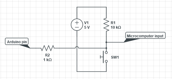
The input pin normally resides at 5V, and is pulled down to GND when the button is pressed. Our own controller (e.g. Arduino) must simulate these button presses whilst allowing normal control via the front panel when desired. This is achieved by using a tristate output which is normally high-impedance and driven low when the remote control command is received. After adding a 1k resistor in series (not strictly necessary and just for protection in case a software bug allows the Arduino output to be driven high), the circuit for each pin looks like this:

Button circuit with Arduino connection

And the function to control the pins looks like this:

void pulsePin(uint_fast8_t pin) {
  if (pin != pin_invalid) {
    pinMode(pin, OUTPUT);
    delay(pin_mark_time);
    pinMode(pin, INPUT);
  }
}

The pin is driven low for pin_mark_time then tristated. The value of pin_mark_time (in milliseconds) can be found by experimentation. In this case, 100ms worked fine.

The Arduino microcontroller can now control the tape deck, but the remote control still needs to be added.

Infrared remote interface

For the remote control, six redundant buttons on the hi-fi amplifier remote (originally for a CD player which I don't have) which roughly correspond to the six buttons on the cassette deck shall be used.

Remote control buttons

A standard 38kHz IR remote control receiver module is hooked up to an oscilloscope and the waveform is examined to determine the protocol. In the image below, the "Play" button is pressed. The waveform is compared to the example waveforms for various popular remote control protocols that are available online.

RC-5 waveform

The protocol turns out to be the very popular RC-5 protocol and five of the six buttons correspond to the standard RC-5 commands for CD players:

  • Reverse: 33
  • Forward: 32
  • Stop: 54
  • Play: 53
  • Pause: 40
  • Sound Mode: 130

The popularity of the Arduino system means an open-source library is available for almost any IR protocol, so a simple RC-5 library is selected for this project. The library is licensed under the permissive 2-clause BSD license. The included code example which prints received codes via the UART confirms the command codes listed above, so all that's left is to pulse the output pins when the appropriate code is received.

In addition to the command code, the RC-5 packet also includes an address, which the library decodes as well. The address allows multiple devices of different types to use the RC-5 protocol without interference. Unsurprisingly, it's the standard CD player address (system 20).

Putting it all together

The full code for the Arduino-based IR cassette deck controller is on my GitHub along with some comments which explain how the code works.

All that remains is to transfer the design to some permanent hardware. I chose to build the final version of the design directly on stripboard instead of using an Arduino plus a shield to make the solution more compact and make it easier to integrate it into the equipment.

An ATmega328p with the Arduino bootloader is used. It could be ported to a smaller microcontroller to make it even more compact, but I didn't perceive the effort as being worth it for this one-off case, so I stuck with the ATmega328p. The necessary components are soldered to the stripboard along with wires to connect it to the "microcomputer PCB" of the cassette deck. The buttons all share a single connector, so the soldering is neat and tidy here. Power is also taken from the microcomputer PCB. The stripboard assembly is mounted on a convenient ledge using hot glue.

Close-up view of the stripboard assembly
View of the inside of the Yamaha K-220 cassette deck with the infrared remote control mod added

Finally, the infrared sensor needs to be placed somewhere. As the cassette deck was not originally designed for a remote control, there is no official place on the front panel for it, but through careful positioning, it is possible to install it without needing to cut any holes without significantly compromising the IR sensitivity.

The IR sensor is installed behind this knob. Whilst refitting the knob does affect the sensitivity somewhat, the sensitivity is still good.

Knob removed showing the position of the IR receiver
Knob refitted, hiding the IR sensor

Saturday, July 11, 2020

VHDL Teletext Decoder Part 3: Data recovery, processing and page extraction

In Part 2, I designed a display controller which can display a 40 character by 25 line screen of text and graphics as used by Teletext (and Mode 7 on the BBC Micro). The display controller reads from a dual-port RAM, which means it can be used in any FPGA project where data display and basic graphics are required. In the case of a teletext decoder, the VBI data needs to be extracted from the composite video signal, error correction needs to be applied, and then the data relating to the currently selected page number needs to be loaded into the dual-port RAM so that it is displayed by the display controller.

RTL block diagram

The teletext decoder section of the design has been broken up into four modules:

  • TXT_DATA_RECOVERY: Detects the start of a packet (line) of teletext data and extracts the serial data
  • TXT_DESERIALISER: Converts the serial data to parallel
  • TXT_DATA_PROCESSOR: Performs error correction on the data and determines the page number and subcode of each packet received
  • TXT_MEMORY_CONTROLLER: Writes packets from the selected page number to the dual-port RAM

Parallel vs serial transmission schemes

Not to be confused with serial and parallel data, these terms refer to the order in which pages are transmitted in the VBI (Vertical Blanking Interval).

In a parallel mode scheme, a few lines from one page in a particular magazine are transmitted followed by a few lines from a page from another magazine and so on. This approach was favoured by UK broadcasters when teletext was broadcast here and is still used by TEEFAX. This scheme can be identified from the display of page numbers only from the current magazine in the rolling header when waiting for a page.

In a serial mode scheme, all packets transmitted belong to the page number and magazine of the last header packet transmitted. This approach is favoured by international broadcasters, and is identified by page numbers from every magazine being displayed in the rolling header.

More detailed information about these schemes is described in Annex B of ETSI EN 300 706.

TXT_DATA_RECOVERY

This module detects the start sequence of the packet then forwards the serial data onto the next module. The start of the packet is shown below:

To simplify the design and avoid the need for a high-speed ADC, the packet is simply digitally sampled, which means the module only has a single digital input. A high-speed comparator is the only active semiconductor required, although the user may have to adjust the trimmer pot RV1 when switching sources.

Composite video input and sampling circuit

The comparator converts the analogue signal into a digital signal suitable for the FPGA:

The data recovery module, along with the rest of the teletext decoder section, runs at 27.750MHz, four times the data bit rate. A SI5351 programmable clock source is used to generate this unusual frequency with great accuracy along with the unique video clock required by the VGA controller for each resolution.

There are four sampled bits per data bit (known as 4x oversampling), and the bit rate has a very tight tolerance so there is no need to worry about clock recovery, which simplifies the design a lot. A shift register is continuously fed with the digital data provided by the comparator and a packet is detected once the start sequence is detected in the shift register. One out of every four bits will be sampled during the inter-bit transition, so the comparison is performed using only three sampled bits in every data bit, then the data sent to the next module is recovered from the middle sampled bit of each subsequent data bit.

Start pattern in teletext waveform

The colour burst is not sampled, nor is the video line number counted. These are not necessary for decoding, and the only consequence is the decoder will be capable of receiving anything transmitted otherwise in accordance with the specification which may be rejected by a commercial decoder.

TXT_DESERIALISER

This module converts the recovered data from serial to parallel. The FRAME_VALID_OUT signal indicates the start and end of each packet received to the next module.

TXT_DATA_PROCESSOR

This is the most complex module in the teletext decoder.

Page number detection

The two main types of packet are page header and normal packets. There's also non-displayable packets, but those will be explained later.

Teletext packet types

Every packet contains the magazine number, which is the leftmost digit of the three-digit page number, however, only the header packet contains the remaining two digits of the page number and the subcode. When a parallel transmission scheme is used, pages from different magazines may be transmitted on different lines in the same video frame, which means that the data processor must remember the page number and subcode of the last transmitted header packet for each of the 8 magazines. This is stored in the PAGE_AND_SUBCODE_CACHE whenever a header packet is received and retrieved whenever a packet other than a header packet is received so that the correct page and subcode is always sent to the next module along with the decoded data.

Packet processing

Hamming coding is used to protect certain data such as the page number and subcode to improve the chances of the header packet being decoded correctly in cases of poor reception. This reduces the chance of an incorrect page being loaded on top of the displayed page when a subsequent header packet is incorrectly determined to have the selected page number. Unfortunately, Hamming code dramatically increases the number of bits taken up by each piece of data, so it is only possible to use it for the most important data, and the display data is only protected with a simple parity check with no error correction capability because it is less critical that every display byte is correctly decoded. It should be noted that correct decoding of every single display byte is expected when the signal quality is good and there is no interference.

The parity checking and Hamming decoding is carried out by sub-modules (VHDL components) in TXT_DATA_PROCESSOR.

TXT_MEMORY_CONTROLLER

This module selects the appropriate address in the dual-port RAM to write each packet belonging to the specified page number to, then forwards the packet data on to the dual-port RAM.

It also controls the display of the status line. The last 8 characters should be continuously updated regardless of the magazine of the header row, whilst the rest of the header row should only be updated when waiting for a newly-selected page number ("search mode"), in which case only header rows from the current magazine should be displayed when the pages are transmitted using the parallel transmission mode, and header rows from all magazines should be displayed when pages are transmitted using the serial transmission mode.

This module also extracts the editorial links (also known as Fastext) for the four coloured buttons and the index button from the relevant non-displayable packet.

The 8 characters in the top left corner of the display are called the status characters. These are controlled by the keypad controller, and are used to display the page number and subcode number. The memory controller monitors these characters and updates the dual-port RAM whenever they change. The UPCOMING_FRAME_IN signal ensures that page content updates (which must happen in real-time) are prioritised over updates to the status characters.

The REQ_SUBCODE_SPEC_IN signal is set when the user requires a specific sub-page to be displayed. When the Time-Text button is pressed, the keypad controller sets the REQ_SUBCODE_SPEC_IN signal and the memory controller will then only display pages where both the page number and subpage match the requested values, otherwise the subpage is ignored and all subpages from the current page will be displayed as they are received.

Screenshot of the project in operation

The project can decode pages generated by VBIT2 running on a Raspberry Pi.

Teletext decoder connected to a display, showing a teletext page

Next: Data recovery, processing and page extraction

Large dot matrix clock, timer and scrolling message display

First completed: August 2014. Additional work carried out late 2025/early 2026. Introduction Previously, the author had made a very small ...