Introduction
I've already shown how to add a VGA output to an FPGA, but a HDMI/DVI output is sometimes more useful, as they offer better compatibility with modern displays, and a much higher bit depth (8 bits of colour per channel) is possible without needing to add extra I/O pins for each bit like you would with VGA. I've implemented a HDMI output as part of the VHDL Teletext project, and the main benefit for that project is that the additional colours supported by Level 2.5 teletext can be generated by the FPGA.
HDMI/DVI are very closely related to VGA, the timings are essentially the same, and it is in fact possible to generate VGA and HDMI/DVI from the same internal signals simultaneously. There is very little difference between HDMI and DVI, but DVI is video only, whereas HDMI usually carries audio as well. Generating audio will not be covered in this article, but any HDMI display should be able to accept a signal without audio, so the implementation in this article can be used for both and the only thing that differs is the choice of connector (the electronics are identical). The interface will be referred to as DVI from here on.
How does HDMI/DVI differ from VGA?
DVI is essentially the digital version of VGA. The main features are:
- Analogue video channels are replaced by TMDS-encoded digital channels
- Sync pulses are replaced by special codes that never appear in the active video area
- Timings can be the same as VGA - timings are broadly categorised as "TV timings" and "PC timings"
- Current-mode signalling is used on the hardware level
- Data clock is 10 times the pixel clock, so a high clock speed is needed, but I'll address this issue by using Double Data Rate I/O
This diagram explains how the control signals work for a DVI video signal. Notice how the diagram is very similar to the equivalent diagram for a VGA interface.

"TV timings" vs "PC timings"
Early HDMI TVs usually only support TV timings, and computer monitors and later TVs usually support all timings (computer monitors may not support interlaced timings, but those are outside the scope of this article). Examples of TV timings are 576p (720x576@50Hz), 720p (1280x720@50Hz and 1280x720@60Hz) and 1080p (1920x1080@50Hz and 1920x1080@60Hz) - 720x576@60Hz is not a proper TV timing, and will not be accepted by most older HDMI TVs. Examples of PC timings are 800x600 and 1280x1024, and PC monitors will often accept any clock frequency you make up as long as the refresh rate is within a certain range such as 50Hz to 80Hz. The most common values for the vertical and horizontal front porch, sync, and back porch for your chosen resolution can be found online (e.g. VESA Monitor Timing Standard).
An additional complication that affects TVs is the RGB Range, which can be "Full range" (0 to 255) or "Limited range" (16 to 235). TVs normally use "Limited range", but unless accurate colour is important, this generally doesn't matter for FPGA applications, especially text-only ones. Limited range was originally used for broadcast applications to avoid clipping analogue signals containing overshoots when they are converted to digital, which could introduce artefacts such as ringing if the digital signal is converted back to analogue.
Timings (EDID) can be read from the connected monitor over an I2C connection. The FPGA Teletext board includes the necessary connections to do this, but this hasn't been implemented in the firmware.
The TMDS signal
Digital video data is encoded using a scheme called TMDS (Transition-minimized differential signaling). It is a similar concept to 8B10B encoding, except the goal is to reduce the number of transitions rather than increase them.
The details of the algorithm are contained within the DVI specification, so I won't explain that in great detail. The algorithm is designed to be relatively easy to implement in programmable logic and in ASICs.
Another detail is that current-mode signalling is employed, whereas FPGAs usually have LVDS outputs, which use voltage-mode signalling. A limited selection of FPGAs have CML outputs, but for those which don't, a converter IC such as the PTN3366 can be used. Using LVDS directly will probably work at low resolutions using a short cable, but I wanted to do it properly on the FPGA Teletext PCB, so I used the PTN3366.
The code
The code is made up of these main parts:
- Port definitions: the input for each channel is 8 bits, but if the input signal uses fewer bits, you can simply duplicate the bits to generate 8 bits for each channel. VHDL Teletext offers the user choice of two resolutions, so a selector input is provided for that. Pixel clock and high-speed clocks (5x pixel clock) are required.
- Counter: controls the active area and pixels
- Sync generator: determines whether the HSync, VSync, both, or no sync control codes should be used according to the counter values and resolution selection
- TMDS encoders: three identical encoders for the three channels
- Shifter: serialises the TMDS data using the high-speed clock
High-speed serialiser
The shifter is the part which differs from most HDMI implementations - the shifter is a shift register which shifts two bits per clock cycle, and two bits are extracted from each shift register to feed to the FPGA pins - this is for the Double Data Rate I/O.

Shifting two bits per clock cycle allows the high-speed clock to be halved compared to the conventional method, which allows a dramatic increase in the maximum resolution without breaking the FPGA's maximum clock speed limit (402.5MHz for the PLL output on the MAX 10). This allows an increase in the maximum resolution from 800x600 to 1280x720. Even if the higher resolutions are not required, this still makes timing closure much easier, so is well worth doing regardless of what resolution you want to use. The impact on power consumption is minimal.
The values in the datasheet under "True LVDS Transmitter Timing Specifications" should also be considered. In the case of the VHDL Teletext board, the FPGA has a limit of 640Mbps, and 1280x720@50Hz is under this limit, but 1280x720@60Hz is above this limit. 1280x720@60Hz is under the limit of the fastest speed grade, which is more expensive. In practice, 1280x720@60Hz works fine on the slower speed grade, but this may not hold true at temperature extremes! The data rate in Mbps is 10 times the pixel clock, even when using DDRIO.
Implementation on the MAX 10 FPGA
On the MAX 10, the GPIO Lite IP core is used to implement Double Data Rate I/O. On other FPGAs, a different IP core may be used, such as the ALTDDIO IP core. The IP core updates the I/O pin on both edges of CLK_VIDEO_BIT, with either bit 0 or bit 1 from the TMDS encoder's shift register selected depending on whether the edge was a rising edge or a falling edge.
Take care when specifying the input pins. On the GPIO Lite IP core, the correct order (from high to low) is the four upper bits (CLK_OUT(1), R_OUT(1)...) followed by the four lower bits (CLK_OUT(0), R_OUT(0)...). This wasn't clearly explained in the documentation and caught me out the first time!
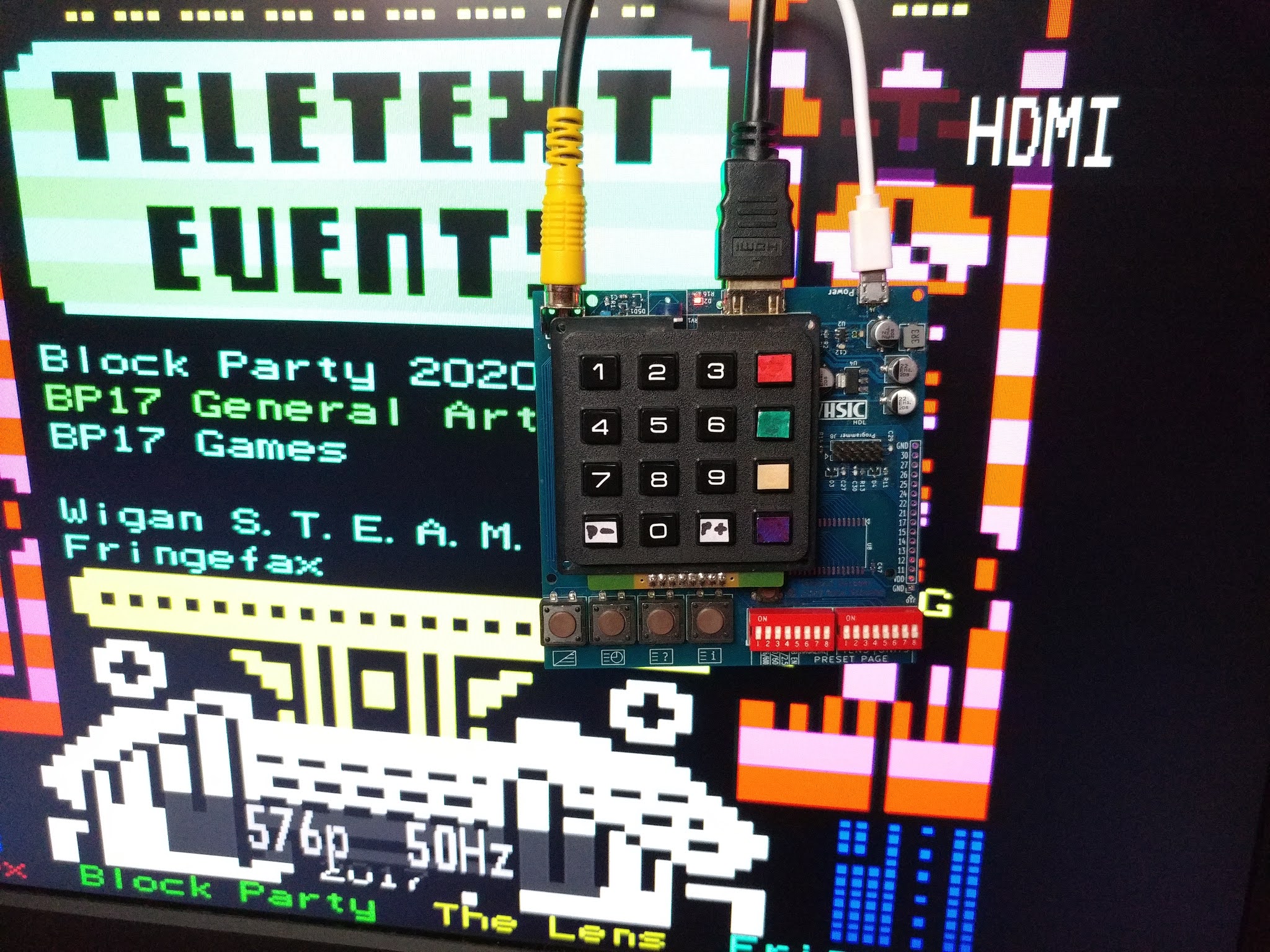
Example output on real hardware
Captured using the FPGA Teletext PCB:

The hardware
The FPGA Teletext PCB, shown below with the numeric keypad removed, is a custom-designed PCB containing all the necessary hardware to decode the teletext data in a composite video signal (from a Raspberry Pi running vbit2 or from a satellite receiver) and display it on a HDMI or DVI display. The firmware could be used on other FPGA boards if the necessary external hardware is added.
Please see the project overview for more details of the hardware, including links to buy.


